Electronic type voltage transformer
A voltage transformer and electronic technology, applied in the direction of inductors, transformers, voltage/current isolation, etc., can solve the problems of measurement accuracy dependent on compensation and adjustment, measurement accuracy seriously affected by temperature, and unsatisfactory linearity
- Summary
- Abstract
- Description
- Claims
- Application Information
AI Technical Summary
Problems solved by technology
Method used
Image
Examples
Embodiment example 1
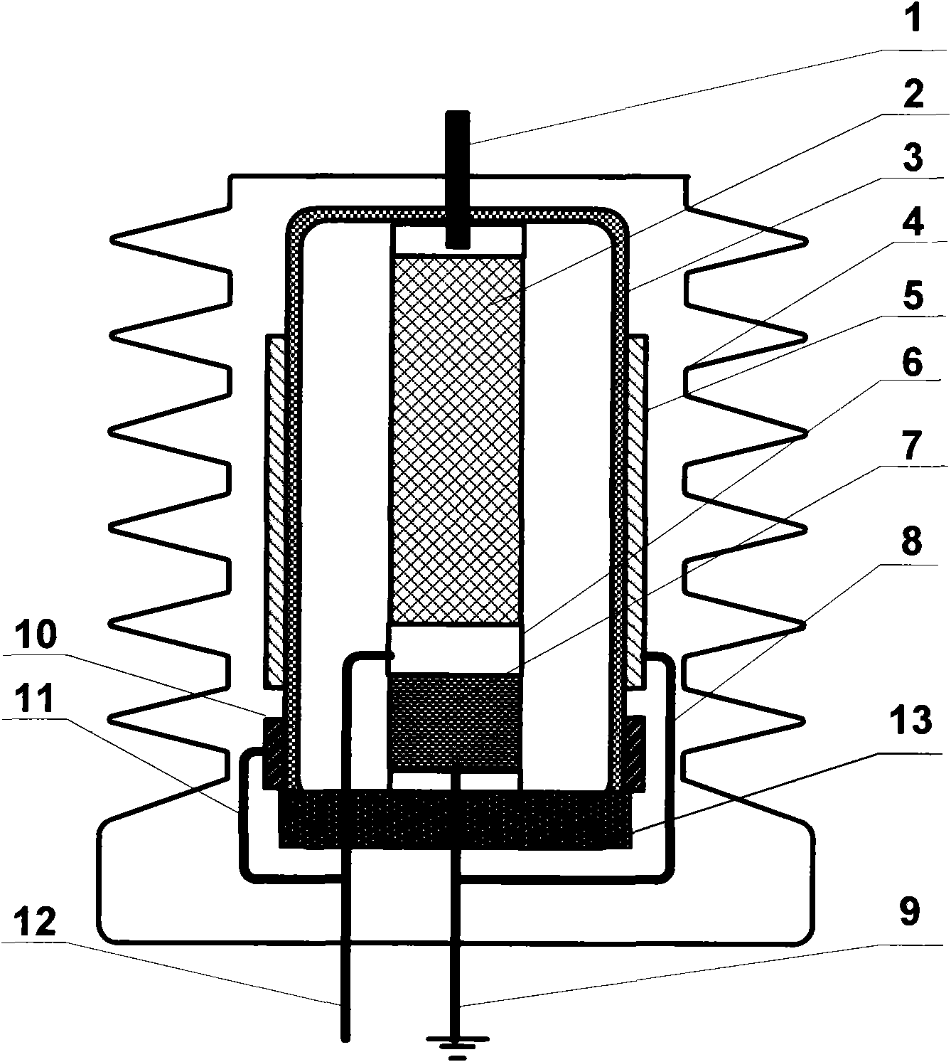
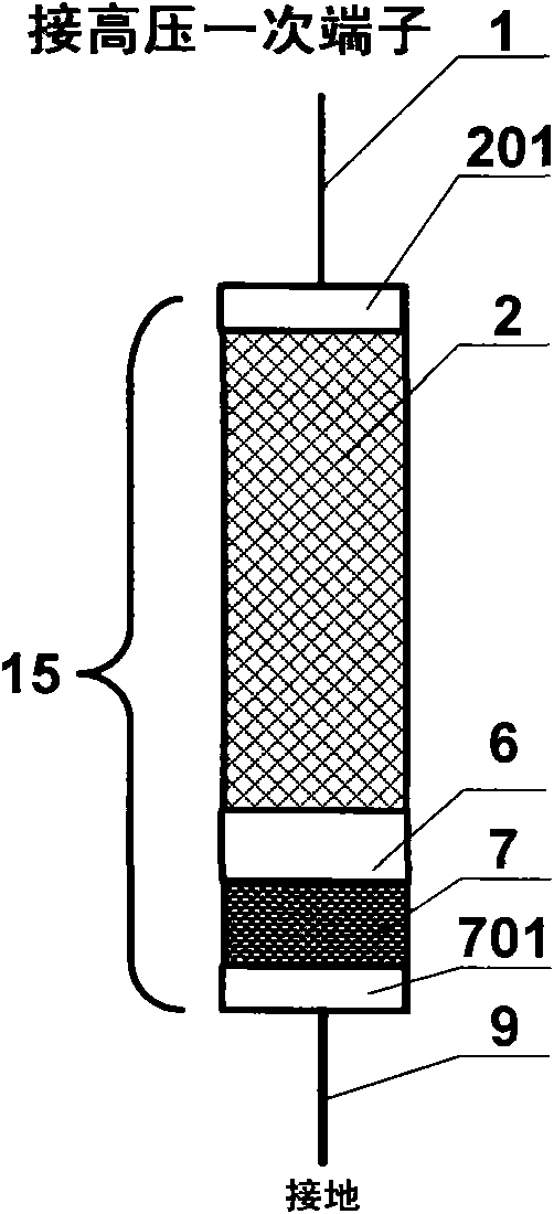
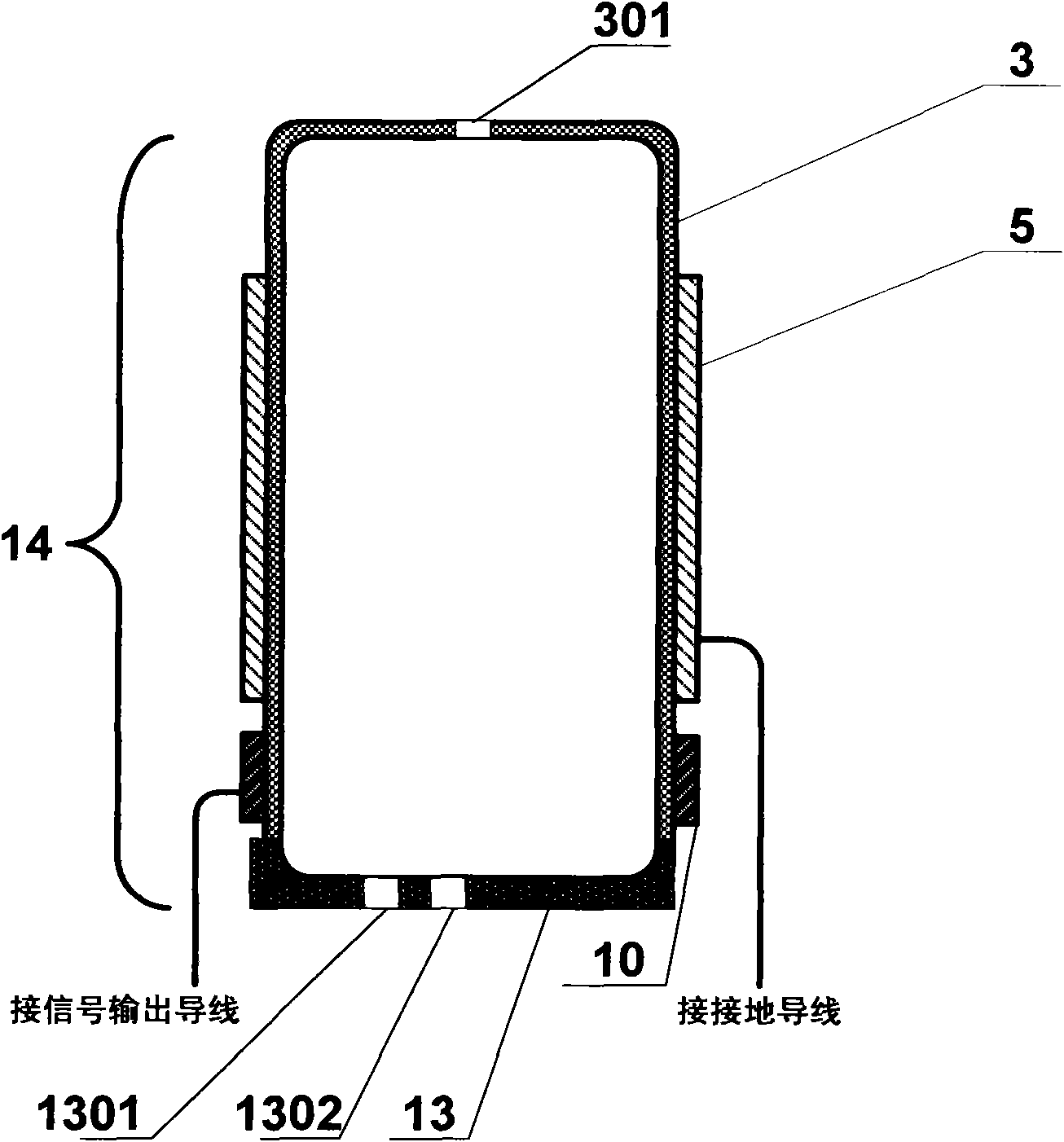
[0024] The specific implementation case 1 of the electronic voltage transformer of the present invention is as figure 1 , figure 2 , image 3 with Figure 4 shown.
[0025] The overall structure of implementation case 1 is as follows figure 1 As shown, a gas (vacuum) shielded cavity structure is adopted. The voltage divider (15) composed of the voltage divider high-voltage arm (2), the signal electrode (6) and the voltage divider low-voltage arm (7) connected in sequence is fixed on the insulating cup (3) with the opening downward and the bottom upward ) and is located on the central axis of the insulating cup (3), the high-voltage wire (1) enters the inner cavity of the insulating cup (3) and the voltage divider high voltage through the high-voltage outlet hole (301) at the bottom of the insulating cup (3). The high-voltage electrode (201) of the arm (2) is connected, and the signal output wire (12) enters the insulating cup ( 3) The inner cavity is connected to the si...
Embodiment example 2
[0033] The specific implementation case 2 of the electronic voltage transformer of the present invention is as figure 1 , figure 2 , image 3 with Figure 5 shown. The difference between implementation case 2 and implementation case 1 is that in implementation case 1, the shielding layer (10) of the signal output terminal is located under the shielding layer (5) of the grounding terminal, and there is an insulating area not coated with any conductive material or semi-conductive material between the two. isolation; and the signal output terminal shielding layer (10) of the implementation case 2 is embedded in the grounding terminal shielding layer (5), and the insulating ring is isolated by not coating any conductive material or semi-conductive material between the two, such as Figure 5 shown.
PUM
 Abstract
Description
Claims
Application Information
 - R&D Engineer
- R&D Manager
- IP Professional
- Industry Leading Data Capabilities
- Powerful AI technology
- Patent DNA Extraction
Browse by: Latest US Patents, China's latest patents, Technical Efficacy Thesaurus, Application Domain, Technology Topic, Popular Technical Reports.
© 2024 PatSnap. All rights reserved.Legal|Privacy policy|Modern Slavery Act Transparency Statement|Sitemap|About US| Contact US: help@patsnap.com


