
Circuit simulation method of single photon avalanche diode detector

A single-photon avalanche and circuit simulation technology, which is applied in the fields of instruments, electrical digital data processing, and special data processing applications, can solve the problems of complex model circuit structure, poor convergence, and low simulation accuracy

Active Publication Date: 2013-05-22
NANJING UNIV OF POSTS & TELECOMM INST AT NANJING CO LTD
View PDF2 Cites 14 Cited by
  • Summary
  • Abstract
  • Description
  • Claims
  • Application Information

AI Technical Summary

Problems solved by technology

However, there is no mature circuit model on the process line that can be called directly, so designers often use an equivalent circuit instead when it comes to related chip design
The early model only considered the DC characteristics of the device during avalanche, and the simulation accuracy was low. Later, Zappa et al. further considered the AC characteristics of the device and proposed a SPICE model with higher accuracy, but the structure of the model circuit was complicated. Many of the component parameters are not easy to determine, and the convergence is not good in actual operation

Method used


Image

  • Circuit simulation method of single photon avalanche diode detector
  • Circuit simulation method of single photon avalanche diode detector
  • Circuit simulation method of single photon avalanche diode detector

Examples


Embodiment Construction

[0030] 1. Model circuit structure

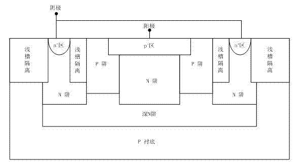
[0031] The invention proposes a circuit simulation method of a single photon avalanche diode (SPAD) detector. figure 1 It is a schematic diagram of the structure of a typical SPAD device, and an avalanche diode is formed between the P+ layer and the N well region. In order to prevent permanent breakdown at the edge of the PN junction under strong reverse bias, there is a lightly doped P-well and a shallow trench (STI) between the P+ layer and the N well for isolation to reduce the p + The fringing electric field of the n junction.

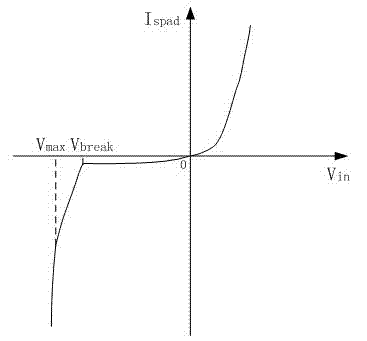
[0032] figure 2 is the current-voltage characteristic curve of SPAD. The working state of the SPAD can be divided into three stages: when the SPAD is forward-conducting, the SPAD can be regarded as an ordinary diode working in the conducting state, and its current value and the voltage drop at both ends of the diode increase exponentially; When the SPAD is reverse-biased and the reverse-bias voltage value at...


PUM


Abstract

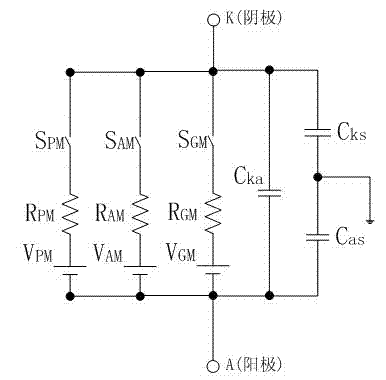
The invention provides a circuit simulation method of a single photon avalanche diode detector. A circuit simulation model structure is composed of a direct current path SRV and an alternating current network knowledge acquisition system (KAS). The direct current path SRV is formed by three branch paths which are in parallel connection. Each branch path is composed of a switch S, a resistor R and a direct current voltage source V which are in series connection. The circuit simulation method comprises the following steps: first, establishing a circuit simulation model for an integrated signaling pathway database (SPAD), accurately describing direct current characteristics, alternating current characteristics and temperature effect of the circuit simulation model, and simulating detection behavior of the SPAD to a single photon. Then, the circuit simulation model achieves by using the model hardware description language Verilog-A and conducts circuit simulation of the SPAD on a universal emulator Cadence. The circuit simulation model accurately simulates the detection behavior of the detector to the single photon by using the circuit model, and the detection behavior includes the direct current characteristics and the alternating current characteristics. The circuit simulation model achieves by using the model hardware description language Verilog-A and has good generality. The circuit simulation model can achieve hybrid simulation of devices and circuits on the universal circuit emulator together with other electronic circuits.

Description

technical field [0001] The invention relates to a circuit simulation method of a single-photon avalanche diode detector. The method uses a circuit model to accurately simulate the detection behavior of the detector to a single photon, including DC characteristics and AC characteristics. The model is realized by using the analog hardware description language Verilog-A, which has good versatility, and can complete the mixed simulation of devices and circuits together with other electronic circuits on a general-purpose circuit simulator. Background technique [0002] Single Photo Avalanche Diode (Single Photo Avalanche Diode, hereinafter referred to as SPAD) is an avalanche photodiode working in Geiger mode. In Geiger mode, the applied working voltage of SPAD is higher than the threshold of avalanche voltage. When SPAD absorbs photons, it immediately releases electron-hole pairs. energy, so as to collide with the crystal lattice and generate new electron-hole pairs. This proce...

Claims


Application Information

Patent Timeline
Patent Type & Authority Applications(China)
IPC IPC(8): G06F19/00
Inventor 徐跃赵菲菲岳恒
Owner NANJING UNIV OF POSTS & TELECOMM INST AT NANJING CO LTD
Learn More