
ESD Protection Components

A technology of electrostatic discharge protection and components, applied in the field of electrostatic discharge protection components, can solve the problem that general products have no structure, diode trigger silicon controlled rectifiers cannot meet the conditions of low leakage current of high-speed transmission components, and do not have NS mode electrostatic discharge protection functions, etc. question

Active Publication Date: 2016-02-24
MACRONIX INT CO LTD
View PDF4 Cites 0 Cited by
  • Summary
  • Abstract
  • Description
  • Claims
  • Application Information

AI Technical Summary

Problems solved by technology

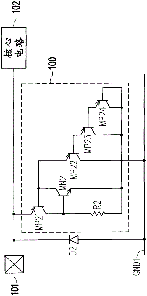
At this time, the equivalent PNP transistors MP22-MP24 in the diode-triggered silicon controlled rectifier 100 will generate a vertical leakage path, which in turn will cause the diode-triggered silicon controlled rectifier 100 to generate a huge leakage current
[0006] In other words, the diode-triggered silicon-controlled rectifier 100 cannot meet the low leakage current requirement required by high-speed transmission devices, and thus cannot be applied to high-speed transmission devices.
In addition, the diode triggered silicon controlled rectifier 100 does not have the ESD protection function of the NS mode
[0007] It can be seen that the above-mentioned existing diode-triggered silicon-controlled rectifier obviously still has inconvenience and defects in structure and use, and needs to be further improved urgently.
In order to solve the above-mentioned problems, the relevant manufacturers have tried their best to find a solution, but no suitable design has been developed for a long time, and the general products do not have a suitable structure to solve the above-mentioned problems. This is obviously related. The problem that the industry is eager to solve

Method used


Image

  • ESD Protection Components
  • ESD Protection Components
  • ESD Protection Components

Examples


Embodiment Construction

[0047] In order to further explain the technical means and effects of the present invention to achieve the intended purpose of the invention, the specific implementation, structure, characteristics and effects of the electrostatic discharge protection element proposed according to the present invention will be described below in conjunction with the accompanying drawings and preferred embodiments. , as detailed below.

[0048] The aforementioned and other technical contents, features and effects of the present invention will be clearly presented in the following detailed description of preferred embodiments with reference to the drawings. Through the description of the specific implementation mode, when the technical means and functions adopted by the present invention to achieve the predetermined purpose can be obtained a deeper and more specific understanding, but the accompanying drawings are only for reference and description, and are not used to explain the present inventi...


PUM


Abstract

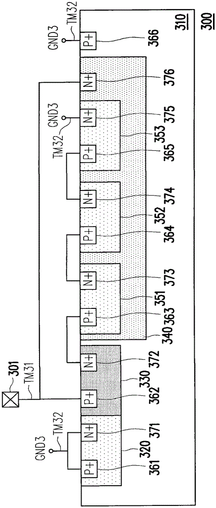
The invention relates to an electrostatic discharge protective element. The electrostatic discharge protective element comprises a P type basement, a plurality of second P type well areas, a plurality of first P + type doped areas and a plurality of N + type doped areas. The P type basement comprises a first P type well area, an N type well area and an N type deep well area. The plurality of second P type well areas are arranged in the N type deep well area. The plurality of N + type doped areas and the plurality of N + type doped areas are alternately arranged in the first P type well area, the N type area and the plurality of second P type well areas The first P + type doped area of the first P type well area is connected with a first connecting end of an electrical connecting element of the N type deep well area. The doped area of the first P type well area is connected with a second connecting end of an electrical connecting element of the P type basement. The plurality of second P type well areas and the plurality of first N + type doped areas inside the plurality of second P type well areas form a diode string. The diode string is connected between the first N + type doped area inside the N type well area and the second connecting end in series.

Description

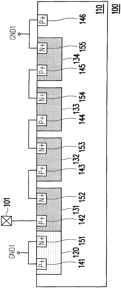
technical field [0001] The invention relates to a protection element, in particular to an electrostatic discharge protection element. Background technique [0002] Electrostatic discharge (ESD) is often the main cause of electrostatic overstress or permanent damage to integrated circuits. Therefore, it is common practice to add electrostatic discharge between the core circuit and the pad. protect components against electrostatic discharge damage. Among many electrostatic discharge protection components, diode-triggered silicon controlled rectifiers (diode-triggered silicon controlled rectifiers, DTSCRs) are widely used in various types of integrated circuits due to their low trigger voltage and fast turn-on characteristics. [0003] figure 1 is a cross-sectional view of a known diode-triggered silicon-controlled rectifier. see figure 1 As shown, the diode triggered silicon controlled rectifier 100 includes a P-type substrate 110 and a P-type well region 120 and N-type we...

Claims


Application Information

Patent Timeline
Patent Type & Authority Patents(China)
IPC IPC(8): H01L27/02H02H9/04
Inventor 何介暐
Owner MACRONIX INT CO LTD
Learn More