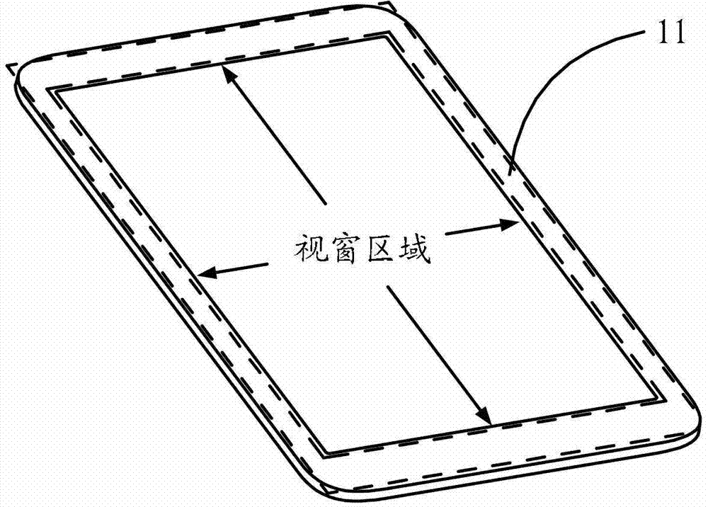
Three-dimensional transparent base material, touch plate, liquid crystal display screen and electronic equipment
A liquid crystal display and transparent substrate technology, which is applied in the fields of electrical digital data processing, optics, instruments, etc., can solve the problem of the area of the screen window occupied by the electrical circuit, and achieve the effect of solving the problem of occupying the area of the screen window.
- Summary
- Abstract
- Description
- Claims
- Application Information
AI Technical Summary
Problems solved by technology
Method used
Image
Examples
Embodiment 1
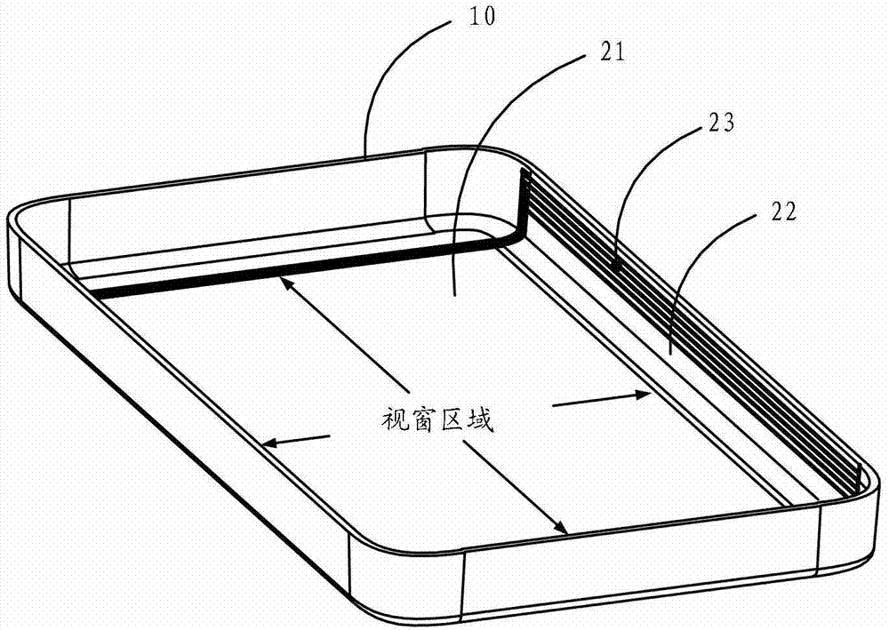
[0031] figure 2 It is a structural schematic diagram of Embodiment 1 of the three-dimensional transparent substrate of the present invention. The three-dimensional transparent substrate 10 is suitable for various electronic devices such as screens, and can be used as an outer layer substrate of TP, or an outer layer substrate of LCD, etc. like figure 2 As shown, the three-dimensional transparent substrate 10 includes a front face 21 and a side elevation 22, wherein the side elevation 22 is provided with electrical circuits 23, such as figure 2 As shown, but not limited thereto, the electrical circuit 23 can be arranged on any one or more side elevations 22 of the three-dimensional transparent substrate 10 according to actual design requirements.
[0032] Specifically, the three-dimensional transparent substrate may be made of glass or plastic. The side elevation 22 refers to a side that is adjacent to and not parallel to the front 21 of the three-dimensional transparent s...
Embodiment 2
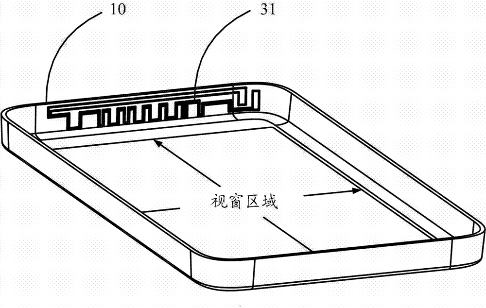
[0040] image 3 It is a schematic structural diagram of Embodiment 2 of the three-dimensional transparent substrate of the present invention. In this embodiment, on the basis of the above-mentioned embodiments, the antenna function of the screen-like electronic device is further implemented by arranging electrical circuits on the side elevation of the inner side of the three-dimensional transparent substrate 10 . Taking the implementation of electrical circuits by ITO sputtering technology as an example, the antenna 31 is fabricated by ITO sputtering technology at the side elevation shown inside the three-dimensional transparent substrate 10 to realize the antenna function. The position of the side elevation forming the antenna 31 is not fixed, and can be arranged on any one or more side elevations of the three-dimensional transparent substrate 10 according to design requirements.
[0041] The three-dimensional transparent base material of this embodiment forms an antenna by ...
Embodiment 3
[0043] Figure 4 It is a schematic structural diagram of the third embodiment of the three-dimensional transparent substrate of the present invention. On the basis of the above-mentioned embodiments, this embodiment further realizes the cable function of the electronic device of the screen by setting the electrical circuit on the side elevation of the inner side of the three-dimensional transparent substrate 10 . Take the realization of electrical circuit by ITO sputtering process as an example. The side facade on the inner side of the three-dimensional transparent substrate 10, such as Figure 4In the position shown, the connection cable 41 is fabricated by the ITO sputtering process to realize the cable function. The side elevation forming the connecting cable 41 is not fixed, and can be arranged on any one or more side elevations of the three-dimensional transparent substrate 10 according to design requirements.
[0044] In the three-dimensional transparent substrate of ...
PUM
 Abstract
Description
Claims
Application Information
 - R&D Engineer
- R&D Manager
- IP Professional
- Industry Leading Data Capabilities
- Powerful AI technology
- Patent DNA Extraction
Browse by: Latest US Patents, China's latest patents, Technical Efficacy Thesaurus, Application Domain, Technology Topic, Popular Technical Reports.
© 2024 PatSnap. All rights reserved.Legal|Privacy policy|Modern Slavery Act Transparency Statement|Sitemap|About US| Contact US: help@patsnap.com


