
Chip sorting library and its pick-and-place mechanism and buffer area planning method for chip sorting library

A buffer area and chip technology, applied in storage devices, conveyor objects, transportation and packaging, etc., can solve problems such as poor scalability, increased load, complex layout, etc., and achieve high work efficiency, simple structure, and expanded capacity.

Inactive Publication Date: 2015-11-25
广东志成华科光电设备有限公司
View PDF6 Cites 0 Cited by
  • Summary
  • Abstract
  • Description
  • Claims
  • Application Information

AI Technical Summary

Problems solved by technology

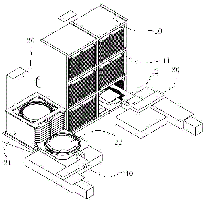
Generally speaking, both the sorting (Bin) library 10 and the wafer (wafer) library 20 are attached with X-direction and Z-direction motion axes to realize the pick-and-place of all sorting trays 12 or wafers 22. This mechanism design exists as follows Several problems: firstly, the separate design of the above-mentioned classification library 10 and wafer library 20 makes the mechanism too complicated and the layout is relatively complicated, and also reduces the interchangeability between the classification cassette 11 and the wafer cassette 21; secondly, The sorting (Bin) library 10 and the wafer (wafer) library 10 themselves need to move as a whole, and will carry all the sorting trays 12 or wafers 22 on them during the movement, so that the moving bin 10 and the wafer library 20 The load increases, and the scalability is poor, the storage capacity cannot be expanded, and it is not convenient for large-scale application and promotion in the industry

Method used


Image

  • Chip sorting library and its pick-and-place mechanism and buffer area planning method for chip sorting library
  • Chip sorting library and its pick-and-place mechanism and buffer area planning method for chip sorting library
  • Chip sorting library and its pick-and-place mechanism and buffer area planning method for chip sorting library

Examples


Embodiment Construction

[0045] The present invention will be described in further detail below in conjunction with the embodiments and accompanying drawings, but the embodiments of the present utility model are not limited thereto.

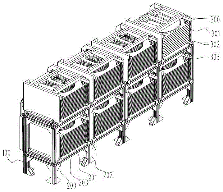
[0046] See figure 2 , the present invention provides a chip sorting library, comprising a bracket 100, a chip sorting cassette 200 and a chip storage cassette 300, the chip sorting cassette 200 and the chip storage cassette 300 are fixed on the bracket 100, and the chip sorting cassette 200 is set There is a slot 202 for fixing the chip sorting tray 201, and the chip sorting tray 201 is fixed in the chip sorting cassette 200 through the slot 202; the chip storage cassette 300 is provided with a slot 302 for fixing the chip storage tray 301, and the chip storage tray 301 is fixed in the chip storage cassette 300 through the card slot 302; the structure of the chip sorting cassette 200 is the same as that of the chip storage cassette 300, and the external dimensions of th...


PUM


Abstract

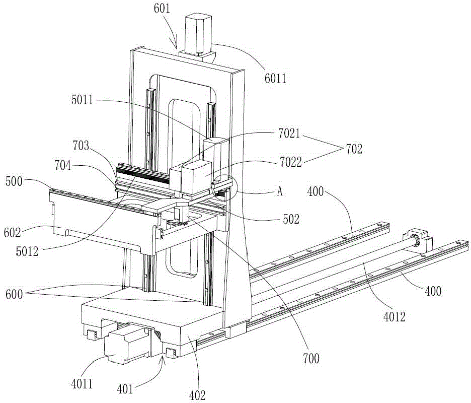
The invention discloses a chip grading library and a picking and placing mechanism thereof and a cache region planning method of the chip grading library. According to the chip grading library, a chip grading box and a chip storing box are fixedly arranged on the same bracket to form an integrated library structure, the integrated library structure is matched with the corresponding picking and placing mechanism so that storage and automatic feeding and discharging of a grading disk and chips are realized; and the grading mechanism has the advantages of stability, expandability, interchangeability of the boxes, and the like. The picking and placing mechanism provided by the invention is placed on one side of the chip grading library, is used for picking and placing the chip grading disk or chip storing disk from the chip grading box or chip storing box through a clamping jaw mechanism through movements on X, Y and Z-axis directions, and has the advantages of simple structure and high working efficiency. The cache region planning method of the chip grading library overcomes the defects of the prior art by mainly using a method of arranging an empty card slot. The slot capacity can be effectively utilized and the capacity of the chip grading library is enlarged.

Description

technical field [0001] The invention relates to the technical field of chip sorting devices, in particular to a chip sorting library, a pick-and-place mechanism thereof, and a buffer area planning method for the chip sorting library. Background technique [0002] In the LED industry, due to the limitation of grinding and cutting in the chip manufacturing process and the growth of epitaxial wafers, a large number of chips formed after cutting the same wafer have different characteristics such as dominant wavelength (peaklength), luminous intensity (MCD), and color temperature (colortemperature). , Operating voltage (V f ) and other photoelectric performance parameters have great inconsistency. Therefore, it is necessary to detect and classify chips according to their photoelectric performance parameters and group similar chips together. [0003] The function of LED chip sorting equipment is to realize the orderly placement of chips of the same category on the same bin accor...

Claims


Application Information

Patent Timeline
Patent Type & Authority Patents(China)
IPC IPC(8): B65G1/04B65G47/90
Inventor 龚时华吴涛贺松平朱文凯朱国文李斌吴磊王瑞
Owner 广东志成华科光电设备有限公司
Learn More