Thin film solar cell back counter electrode and preparation method thereof
A technology of solar cells and counter electrodes, which is applied in the manufacture of circuits, electrical components, and final products. It can solve the problems of poor conductivity of the back and counter electrodes, contradictions between electrical and optical properties, etc., to improve efficiency, improve lateral conductivity, Reduce the effect of spreading
- Summary
- Abstract
- Description
- Claims
- Application Information
AI Technical Summary
Problems solved by technology
Method used
Image
Examples
preparation example Construction
[0027] The preparation method of the back electrode of the thin film solar cell of the present invention comprises the following steps
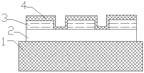
[0028] (1) Clean the substrate 1 and dry it with high-purity nitrogen gas, then place it in a magnetron sputtering growth chamber, and deposit a continuous metal film 2 on the substrate 1 by magnetron sputtering technology, the metal film 2 The thickness is 60nm-400nm, the substrate 1 is polished glass, single crystal silicon wafer, ceramic sheet or metal resistant to 500°C high temperature, the metal film 2 is Ag film, Cu film or Al film, the background vacuum of the sputtering chamber The degree is 5.0×10 -4 Pa~8.0×10 -4 Pa, the substrate temperature is 25°C-500°C, the sputtering process is carried out in low-pressure high-purity argon, the pressure is kept at 1Pa-2Pa, the sputtering power is 30W-50W, and the deposition time is 1min-10min;
[0029] (2) Fix the metal mask with the grid pattern on the surface of the metal film 2, and place ...
Embodiment 1
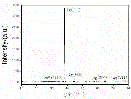
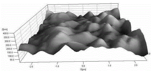
[0033] Such asfigure 1 As shown, the back electrode of a thin-film solar cell includes polished glass resistant to a high temperature of 500°C as a substrate 1, and a metal film 2 with a thickness of 60 nm is deposited on the surface of the substrate 1. The metal film 2 is an Ag metal film, and the surface of the Ag metal film is deposited with The first transparent conductive film 3 of the 20nm thick grid pattern, the first transparent conductive film 3 is an ATO grid pattern transparent conductive film, and the grid spacing is 10 μ m, and the second transparent conductive film with a thickness of 1 nm is also deposited on the ATO mesh pattern transparent conductive film. The film 4, the second transparent conductive film 4 is an ATO transparent conductive film. After testing, the average haze value of the back-to-back electrode described in Example 1 in the visible light and infrared bands is above 95%, and the value of the lateral transmission resistivity is 1.248×10 -6 Ω·c...
Embodiment 2
[0040] The back electrode of the thin-film solar cell includes a polished single-crystal silicon wafer resistant to 500°C high temperature as the substrate 1, a metal film 2 with a thickness of 250nm is deposited on the surface of the substrate 1, the metal film 2 is a Cu metal film, and the surface of the Cu metal film is deposited with The first transparent conductive film 3 of 100nm thick grid form, the first transparent conductive film 3 is AZO grid form transparent conduction film, grid spacing is 500 μ m, the second transparent conduction film of 5nm thickness is also deposited on the AZO grid form transparent conduction film The film 4, the second transparent conductive film 4 is an AZO transparent conductive film. After testing, the average haze value of the back-to-back electrode described in Example 1 in the visible light and infrared bands is above 95%, and the value of the lateral transmission resistivity is 1.521×10 -6 Ω·cm , the vertical transmission resistivity ...
PUM
| Property | Measurement | Unit |
|---|---|---|
| Thickness | aaaaa | aaaaa |
| Thickness | aaaaa | aaaaa |
| Thickness | aaaaa | aaaaa |
Abstract
Description
Claims
Application Information
 - Generate Ideas
- Intellectual Property
- Life Sciences
- Materials
- Tech Scout
- Unparalleled Data Quality
- Higher Quality Content
- 60% Fewer Hallucinations
Browse by: Latest US Patents, China's latest patents, Technical Efficacy Thesaurus, Application Domain, Technology Topic, Popular Technical Reports.
© 2025 PatSnap. All rights reserved.Legal|Privacy policy|Modern Slavery Act Transparency Statement|Sitemap|About US| Contact US: help@patsnap.com


