Memory chip erasing method

A memory chip and storage unit technology, applied in static memory, read-only memory, information storage, etc., can solve the problems of shortening erasing time and long erasing method, and achieve shortening erasing time, reliability assurance, and ease of use. effect achieved

Inactive Publication Date: 2013-03-27
INST OF MICROELECTRONICS CHINESE ACAD OF SCI
View PDF4 Cites 5 Cited by
  • Summary
  • Abstract
  • Description
  • Claims
  • Application Information

AI Technical Summary

Problems solved by technology

[0012] Aiming at the problem that the time of the existing erasing method is too long, the main purpose of the present invention is to provide a method for erasing the memory chip to shorten the erasing time and ensure the reliability of the chip

Method used


Image

  • Memory chip erasing method
  • Memory chip erasing method
  • Memory chip erasing method

Examples


Embodiment Construction

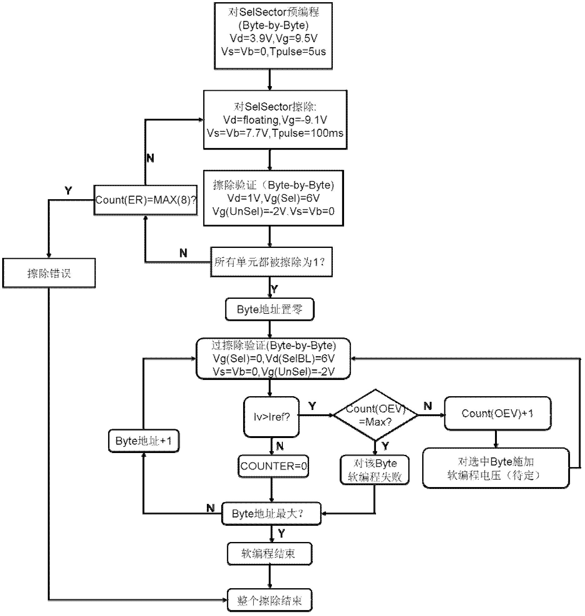
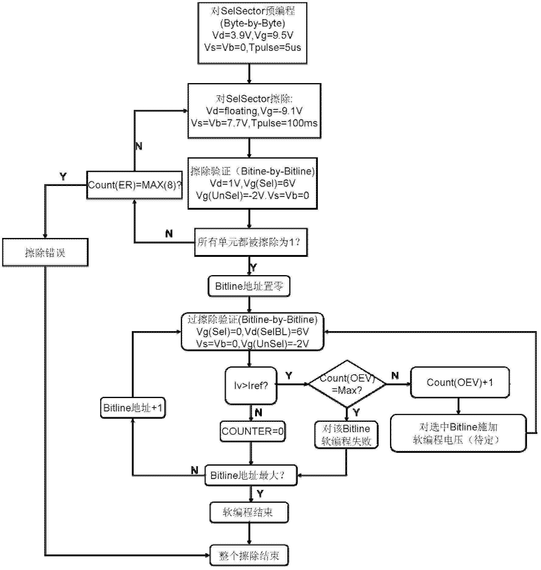
[0027] In order to make the object, technical solution and advantages of the present invention clearer, the present invention will be described in further detail below in conjunction with specific embodiments and with reference to the accompanying drawings.

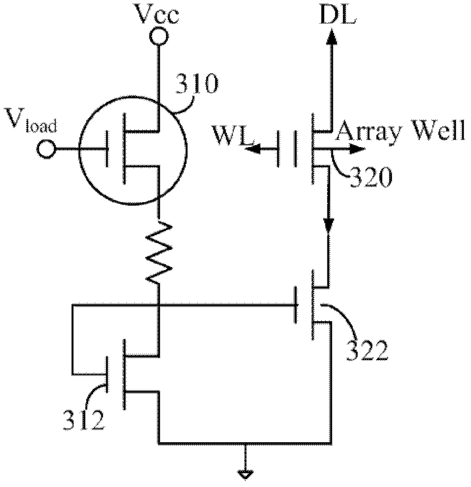
[0028] The method for erasing a memory chip proposed by the present invention, its basic idea is all aimed at a bit line (Bit line) when erasing verification, soft programming and soft programming verification, and the common source of the memory chip is grounded. Connecting to the current limiting device specifically includes: pre-programming the blocks in the memory cells; erasing all the memory cells; verifying the memory cells after erasing; and performing soft programming verification in units of bit lines.

[0029] In order to damage the unit and circuit due to the excessive current flowing through the memory cell during erasing verification and soft programming verification, a current limiting device is added to the...


PUM


Abstract

The present invention discloses a memory chip erasing method, wherein a current limiting device connection manner of a common-source of a memory chip is changed into a ground connection manner. The method comprises: carrying out pre-programming on a block in a storage unit; erasing all storage units; verifying the erased storage unit; and adopting a bit line as a unit to carry out soft programming verification. With the method, an erasing time can be effectively shortened; due to use of the current limiting device, a plurality of the units are concurrently erased, and the current of the storage unit can not be too large, such that the storage unit can not be destroyed, and reliability of the erasing operation is ensured, such that the method is particularly applicable for large capacity memory chips.

Description

technical field [0001] The invention relates to the technical field of integrated circuits and nonvolatile memory chips, in particular to a method for erasing memory chips. Background technique [0002] Non-volatile memory is a rapidly developing field. Most storage devices used in non-volatile memory chips now use floating gate structure storage devices, and erasing the floating gate structure storage devices mostly uses electrically erasable Way. During erasing, a negative bias voltage is applied to the floating gate, and a positive bias voltage is applied to the substrate at the same time, thereby removing electrons on the floating gate to realize erasing of the storage device with a floating gate structure. [0003] One problem with erasing floating gate memory devices is over-erasing. When the electrons on the floating gate are removed too much, over-erasing will occur. At this time, there will be a certain amount of positive charge on the floating gate, making the st...

Claims


Application Information

Patent Timeline
IPC IPC(8): G11C16/14G11C16/34
Inventor 刘明陈映平冀永辉谢常青
Owner INST OF MICROELECTRONICS CHINESE ACAD OF SCI
Why Eureka
Try Eureka