Green organic electroluminescent device and fabrication method thereof
An electroluminescent and organic technology, applied in the field of green organic electroluminescent devices and their preparation, can solve the problems of unfavorable device carrier injection, high device operating voltage, affecting device working life, etc. Luminous efficiency, the effect of delaying the decay of efficiency
- Summary
- Abstract
- Description
- Claims
- Application Information
AI Technical Summary
Problems solved by technology
Method used
Image
Examples
preparation example Construction
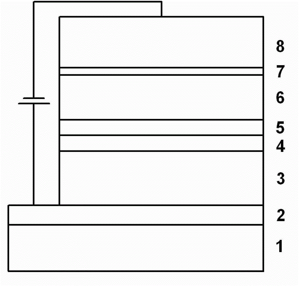
[0063] The present invention also provides a preparation method of a green organic electroluminescence device, comprising:
[0064] forming an anode layer on the substrate;
[0065] A hole-dominated light-emitting layer is formed on the anode layer, and the hole-dominated light-emitting layer is formed by doping a green organic light-emitting material in a hole-type organic host material, and the green organic light-emitting material occupies the hole-type organic host material. The mass percentage of the host material is 5.0%~12.0%, and the green organic luminescent material is tris(2-phenylpyridine)iridium;
[0066] An electron-dominated light-emitting layer is formed on the hole-dominated light-emitting layer, and the electron-dominated light-emitting layer is formed by doping a green organic light-emitting material in an electron-type organic host material, and the green organic light-emitting material occupies the electron-type organic host material. The mass percentage ...
Embodiment 1
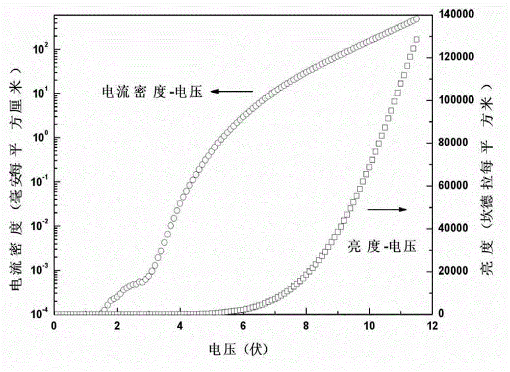
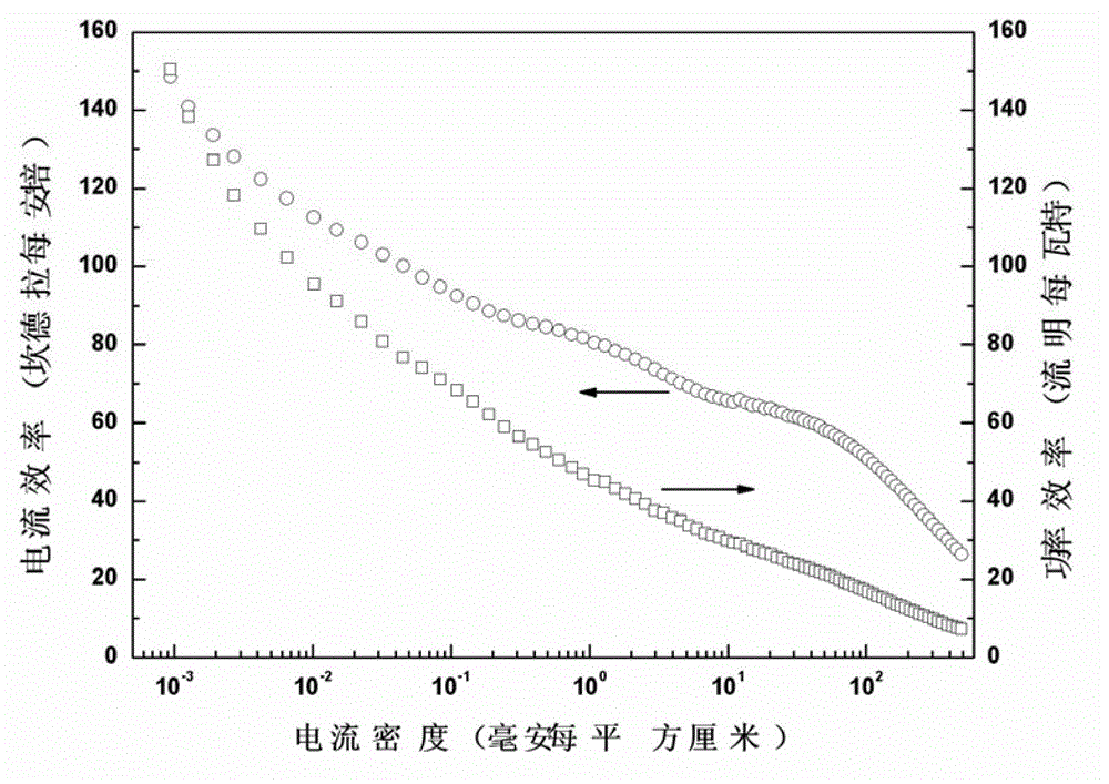
[0092] Glass is used as the substrate; an anode layer of indium tin oxide (ITO) material is formed on the glass substrate, and the anode layer is chemically etched into strip electrodes with a width of 10 mm and a length of 30 mm, and the strip electrodes are cleaned with Ultrasonic cleaning of liquid and deionized water for 15 minutes and drying in an oven. The dried electrode was subjected to low-pressure oxygen plasma treatment with a voltage of 400 volts for 10 minutes on the ITO anode in an atmosphere with a vacuum degree of 10 Pa. Transfer to the organic evaporation chamber, in a vacuum of 1~2×10 -5 In the organic evaporation chamber of Pascal, a 50-nanometer-thick hole-transporting layer was sequentially deposited on the anode layer at a TAPC evaporation rate of 0.05 nm / s, and Ir(ppy) 3 Evaporate 5nm thick Ir(ppy) at 0.006nm / s and MCP at 0.1nm / s 3 Hole-dominated light-emitting layer doped with MCP, Ir(ppy) 3 Evaporate 5nm thick Ir(ppy) at 0.008nm / s and TmPyPB at 0.1nm...
Embodiment 2
[0096] Glass is used as the substrate; an anode layer of indium tin oxide (ITO) material is formed on the glass substrate, and the anode layer is chemically etched into strip electrodes with a width of 10 mm and a length of 30 mm, and the strip electrodes are cleaned with Ultrasonic cleaning of liquid and deionized water for 15 minutes and drying in an oven. The dried electrode was subjected to low-pressure oxygen plasma treatment with a voltage of 400 volts for 10 minutes on the ITO anode in an atmosphere with a vacuum degree of 10 Pa. Transfer to the organic evaporation chamber, in a vacuum of 1~2×10 -5 In the organic evaporation chamber of Pascal, a 50-nanometer-thick hole-transporting layer was sequentially deposited on the anode layer at a TAPC evaporation rate of 0.05 nm / s, and Ir(ppy) 3 Evaporate 8nm thick Ir(ppy) at 0.006nm / s and MCP at 0.1nm / s 3 Hole-dominated light-emitting layer doped with MCP, Ir(ppy) 3 Evaporate 8nm thick Ir(ppy) at 0.008nm / s and TmPyPB at 0.1nm...
PUM
| Property | Measurement | Unit |
|---|---|---|
| Thickness | aaaaa | aaaaa |
| Thickness | aaaaa | aaaaa |
| Thickness | aaaaa | aaaaa |
Abstract
Description
Claims
Application Information
 - R&D
- Intellectual Property
- Life Sciences
- Materials
- Tech Scout
- Unparalleled Data Quality
- Higher Quality Content
- 60% Fewer Hallucinations
Browse by: Latest US Patents, China's latest patents, Technical Efficacy Thesaurus, Application Domain, Technology Topic, Popular Technical Reports.
© 2025 PatSnap. All rights reserved.Legal|Privacy policy|Modern Slavery Act Transparency Statement|Sitemap|About US| Contact US: help@patsnap.com


