Graphene quantum capacity measurement device and preparing method thereof

A technology of capacitance testing and ene quantum, which is applied in the direction of measuring electrical variables, measuring resistance/reactance/impedance, instruments, etc., can solve the problem of large physical thickness, large physical thickness of gate dielectric, increase of equivalent oxide layer thickness of gate oxide layer, etc. problem, to achieve the effect of increasing the specific gravity and improving the accuracy

Active Publication Date: 2014-12-03
TSINGHUA UNIV
View PDF9 Cites 0 Cited by
  • Summary
  • Abstract
  • Description
  • Claims
  • Application Information

AI Technical Summary

Problems solved by technology

[0006] Since there are no dangling bonds and hydrophilic groups on the surface of graphene, direct ALD (atomic layer deposition) cannot be performed, and the method of first depositing metal and then oxidation leads to increased EOT (equivalent oxide thickness) of the gate oxide layer; at the same time, due to The difference in energy band structure, Fowler-Nordheim (Fowler-Nordheim) tunneling is significantly larger than that of silicon semiconductor devices, and the physical thickness of the gate dielectric needs to be very large
Therefore, when using the existing above-mentioned structure, the physical thickness of the gate oxide layer is relatively large, and the capacitance Cox is small, while the quantum capacitance Cq of graphene itself is very large, so the total capacitance measured is mainly composed of the capacitance Cox of the gate oxide layer. decision, leading to the inaccurate quantum capacitance Cq of graphene

Method used


Image

  • Graphene quantum capacity measurement device and preparing method thereof
  • Graphene quantum capacity measurement device and preparing method thereof
  • Graphene quantum capacity measurement device and preparing method thereof

Examples


Embodiment approach

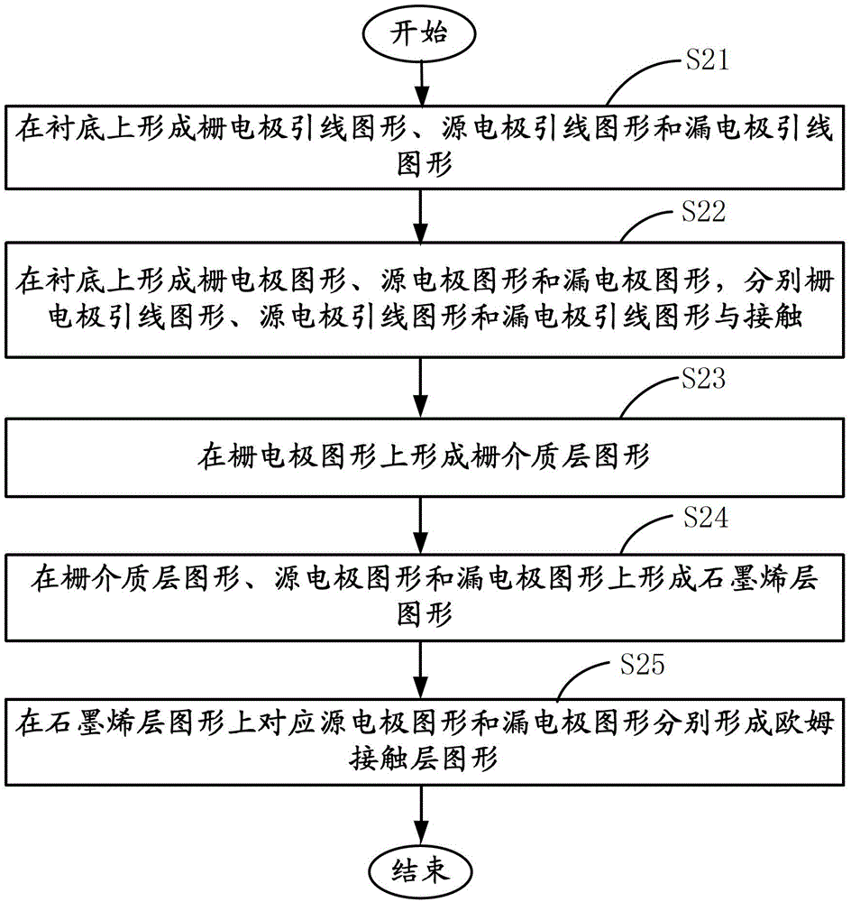
[0058] refer to figure 2 , the present invention also provides a kind of preparation method of graphene quantum capacitor device, and one embodiment thereof comprises:

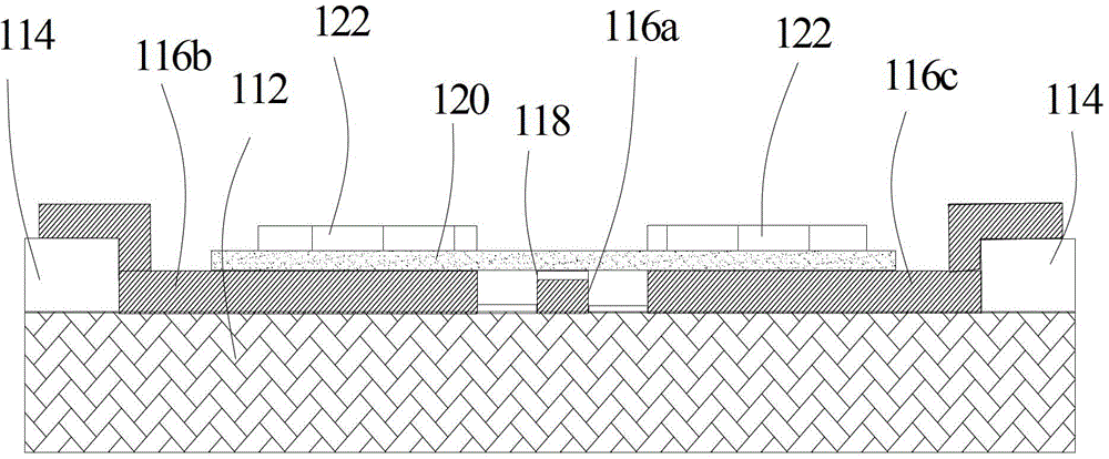
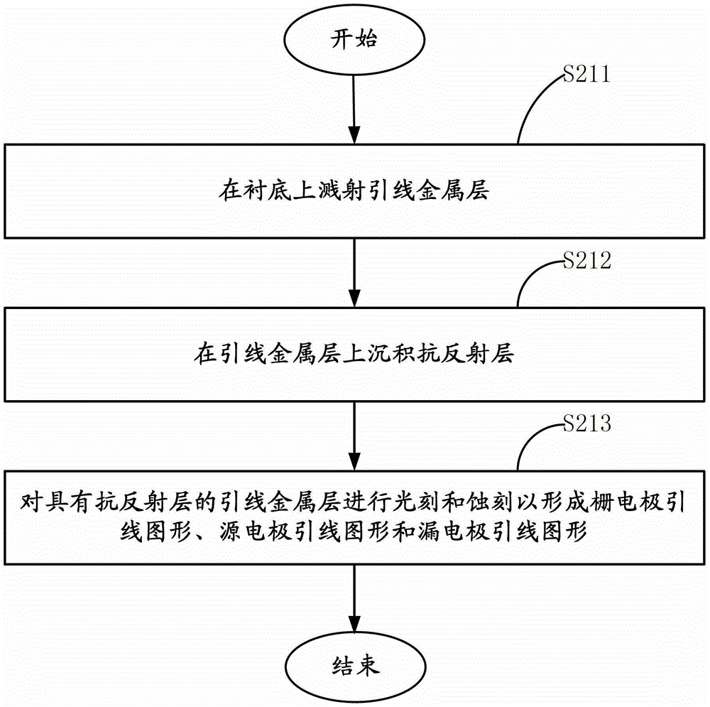
[0059] Metal lead pattern forming step S21: forming a gate electrode lead pattern, a source electrode lead pattern and a drain electrode lead pattern on the substrate. Execution of this step can result in Figure 3A-2 In the shown structure, a source electrode lead pattern 314b and a drain electrode lead pattern 314c are formed on the substrate 312. Since it is a cross-sectional view, the gate electrode lead pattern is not shown in the figure.

[0060] Electrode pattern forming step S22: forming a gate electrode pattern, a source electrode pattern and a drain electrode pattern on the substrate to be in contact with the gate electrode lead pattern, the source electrode lead pattern and the drain electrode lead pattern respectively. Execution of this step can result in Figure 3B-2 In the shown structure, a ...


PUM

PropertyMeasurementUnit
thicknessaaaaaaaaaa
thicknessaaaaaaaaaa
thicknessaaaaaaaaaa

Abstract

The invention relates to a graphene quantum capacity measurement device and a preparing method of the graphene quantum capacity measurement device. The method includes that a gate electrode leading wire pattern, a source electrode leading wire pattern and a drain electrode leading wire pattern are formed on a substrate, a gate electrode pattern, a source electrode pattern and a drain electrode pattern are formed on the substrate and respectively contact the gate electrode leading wire pattern, the source electrode leading wire pattern and the drain electrode leading wire pattern. A gate medium layer pattern is formed on the gate electrode pattern. Graphene layer patterns are formed on the gate medium layer pattern, the source electrode pattern and the drain electrode pattern. Ohmic contact layer patterns which respectively correspond to the source electrode pattern and the drain electrode pattern are arranged on the graphene layer pattern. The graphene quantum capacity measurement device and the preparing method of the graphene quantum capacity measurement device can improve the measurement accuracy of graphene quantum capacity.

Description

technical field [0001] The invention relates to a quantum capacitance testing device, in particular to a graphene quantum capacitance testing device and a preparation method thereof. Background technique [0002] Two-dimensional materials with a single-layer sheet structure composed of carbon atoms, such as graphene, can be used for Fabricate a new generation of semiconductor devices with smaller size and faster conduction speed. [0003] Existing quantum capacitance test device based on graphene, comprises substrate, is formed with graphene, graphene as the channel material of semiconductor device on the substrate, forms source / drain electrode, gate dielectric (gate oxide layer) successively on it ) and the gate electrode. [0004] It can be seen that the quantum capacitance Cq of graphene and the capacitance Cox of the gate oxide layer are in series, and the total capacitance Ctotal is: [0005] Ctotal = 1 ...

Claims


Application Information

Patent Timeline
Patent Type & Authority Patents(China)
IPC IPC(8): G01R27/26
Inventor 肖柯吴华强吕宏鸣钱鹤伍晓明
Owner TSINGHUA UNIV
Why Eureka
Try Eureka