Dual-sided processing method and exposure device
A technology of exposure device and double-sided process, which is applied in photoplate-making process exposure device, micro-lithography exposure equipment, pattern-surface photoplate-making process, etc., can solve the problems of difficult alignment and low product yield, and achieve Improve efficiency, position accuracy, and ensure quality
- Summary
- Abstract
- Description
- Claims
- Application Information
AI Technical Summary
Problems solved by technology
Method used
Image
Examples
Embodiment Construction
[0032] The specific implementation manner of the present invention will be described in detail below in conjunction with the accompanying drawings.
[0033] In the existing double-sided process, it is difficult to identify the substrate alignment mark, and the yield rate of the finished product is low. Therefore, in order to solve this problem, the present invention designs the exposure device for the double-sided process. Alignment processing, and then the double-sided graphics of the substrate are made separately.
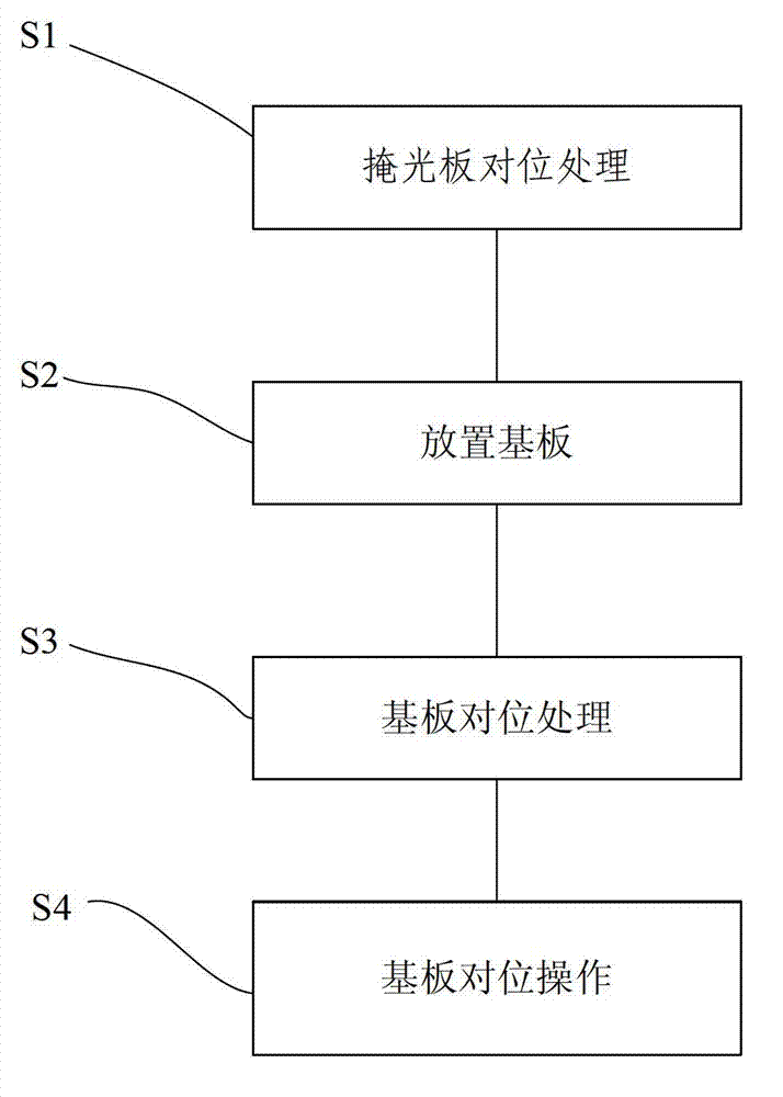
[0034] This embodiment provides a double-sided process method and exposure device in the manufacturing process of semiconductors and liquid crystal displays. During the exposure operation, such as figure 1 and figure 2 As shown, the double-sided process method comprises the following steps:
[0035] S1: according to actual needs, perform alignment processing on the two photomasks 1 used in the double-sided manufacturing process.
[0036] The alignment process...
PUM
 Abstract
Description
Claims
Application Information
 - R&D
- Intellectual Property
- Life Sciences
- Materials
- Tech Scout
- Unparalleled Data Quality
- Higher Quality Content
- 60% Fewer Hallucinations
Browse by: Latest US Patents, China's latest patents, Technical Efficacy Thesaurus, Application Domain, Technology Topic, Popular Technical Reports.
© 2025 PatSnap. All rights reserved.Legal|Privacy policy|Modern Slavery Act Transparency Statement|Sitemap|About US| Contact US: help@patsnap.com


