N-type silicon substrate based back contact type HIT (Heterojunction with Intrinsic Thin layer) solar cell structure and preparation method thereof

A back-contact solar cell technology, applied in circuits, photovoltaic power generation, electrical components, etc., can solve problems such as reducing the efficiency of sunlight utilization, and achieve the effects of avoiding shading, improving efficiency, and simple preparation process

Inactive Publication Date: 2013-02-13
山东力诺太阳能电力股份有限公司
View PDF5 Cites 14 Cited by
  • Summary
  • Abstract
  • Description
  • Claims
  • Application Information

AI Technical Summary

Problems solved by technology

But it needs to print metal electrodes on the front side, which significantly reduces the utilization efficiency of sunlight

Method used


Image

  • N-type silicon substrate based back contact type HIT (Heterojunction with Intrinsic Thin layer) solar cell structure and preparation method thereof
  • N-type silicon substrate based back contact type HIT (Heterojunction with Intrinsic Thin layer) solar cell structure and preparation method thereof
  • N-type silicon substrate based back contact type HIT (Heterojunction with Intrinsic Thin layer) solar cell structure and preparation method thereof

Examples


Embodiment 1

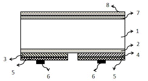
[0032] Refer to the accompanying drawings in the manual figure 1 , N-type silicon substrate 1 light-receiving surface from the inside to the outside is the light-receiving surface n-type amorphous or microcrystalline silicon layer 7, anti-reflection layer 8; the backlight surface is the intrinsic amorphous or microcrystalline silicon layer from the inside to the outside 2. There is an interval between the p-type amorphous or microcrystalline silicon layer 3 and the n-type amorphous or microcrystalline silicon layer 4 on the backlight surface and are alternately arranged on the intrinsic amorphous or microcrystalline silicon layer 2, and the p-type amorphous or microcrystalline silicon layer 2 Both the microcrystalline silicon layer 3 and the n-type amorphous or microcrystalline silicon layer 4 on the backlight surface are covered with a transparent conductive film 5 , and the metal electrode 6 is located on the transparent conductive film 5 .

[0033] p-type amorphous or micr...


PUM

PropertyMeasurementUnit
Thicknessaaaaaaaaaa

Abstract

The invention relates to an N-type silicon substrate based back contact type HIT (Heterojunction with Intrinsic Thin layer) solar cell structure and a preparation method thereof. The structure is characterized in that the illuminated surface of an N-type silicon substrate comprises an illuminated surface n-type amorphous or microcrystalline silicon layer and an antireflection layer from inside to outside in sequence; the shady surface comprises an intrinsic amorphous or microcrystalline silicon layer, a p-type amorphous or microcrystalline silicon layer and a shady surface n-type amorphous or microcrystalline silicon layer from inside to outside in sequence; the p-type amorphous or microcrystalline silicon layer and the shady surface n-type amorphous or microcrystalline silicon layer are separated by an interval and are alternately arranged on the intrinsic amorphous or microcrystalline silicon layer; transparent conducting thin films cover the p-type amorphous or microcrystalline silicon layer and the shady surface n-type amorphous or microcrystalline silicon layer; and metal electrodes are arranged on the transparent conducting thin films. The HIT solar cell structure and the preparation method have the following beneficial effects: in combination with the preparation methods of the conventional crystalline silicon solar cells and the thin film solar cells and relative to the traditional HIT cells, the preparation process is simple, the usage amount of the metal electrodes is reduced, and the problem that the front electrodes of the conventional solar cells shade light is avoided, thus improving the efficiency of the solar cell.

Description

technical field [0001] The invention relates to the technical field of crystalline silicon solar cells, in particular to a structure and preparation method of a back-contact HIT solar cell based on an N-type silicon substrate. Background technique [0002] The rapid development of the solar energy industry requires an industrialized technology with simple process flow and high photoelectric conversion efficiency to reduce the cost of power generation and achieve the goal of being equal to or lower than the price of mains electricity. [0003] With the development of industrialization, the current conventional crystalline silicon cells have made great progress in various aspects such as improvement of conversion efficiency and cost reduction, but their structure and technical characteristics limit the further improvement of their efficiency. As a result, various solutions have emerged in the industry, including selective emitter solar cells, back contact solar cells, HIT ce...

Claims


Application Information

Patent Timeline
IPC IPC(8): H01L31/0747H01L31/0224H01L31/20
CPCY02E10/50Y02P70/50
Inventor 贾河顺姜言森程亮任现坤张春艳孙继峰马继磊徐振华
Owner 山东力诺太阳能电力股份有限公司
Why Eureka
Try Eureka