A kind of crystalline silicon and preparation method thereof

A technology of crystalline silicon and monocrystalline silicon, applied in the field of crystalline silicon and its preparation, can solve the problems of low battery conversion efficiency, affecting the ratio of single crystals, poor quality of silicon blocks, etc., and achieve the improvement of battery conversion efficiency, quality improvement and low cost Effect

Active Publication Date: 2015-08-05
JIANGXI SAI WEI LDK SOLAR HI TECH CO LTD
View PDF3 Cites 0 Cited by
  • Summary
  • Abstract
  • Description
  • Claims
  • Application Information

AI Technical Summary

Problems solved by technology

[0004] However, there is no mature process for the production of quasi-monocrystalline silicon wafers at present. In the prior art, the bottom of the crucible is generally covered with monocrystalline silicon seed crystals (such as figure 1 ), and then filled with silicon material, heated and melted and the temperature at the bottom of the crucible is controlled to prevent the seed crystal from being completely melted, so that the silicon liquid grows on the seed crystal that has not been completely melted, and grows a quasi-single crystal with a single crystal structure
This process not only requires a large amount of seed crystals and high production costs, but also due to the uniformity and orientation of the thermal field, it is difficult to grow single crystals in the area close to the side wall of the crucible, and most areas are polycrystalline areas (such as figure 2 ), severely affects the ratio of single-crystal
Since this area is the coexistence area of ​​single crystal and polycrystalline, the crystal grains are squeezed against each other, and dislocations are easy to expand and proliferate, resulting in poor quality of silicon blocks in this area, and low cell conversion efficiency, even lower than that of ordinary polycrystalline silicon wafers.

Method used


Image

  • A kind of crystalline silicon and preparation method thereof
  • A kind of crystalline silicon and preparation method thereof
  • A kind of crystalline silicon and preparation method thereof

Examples


Embodiment 1

[0036] A method for preparing crystalline silicon, comprising the steps of:

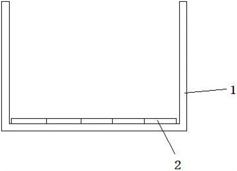
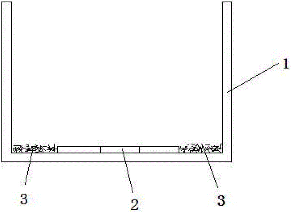
[0037] (1) Randomly lay single crystal silicon seed crystals in the center of the bottom of the crucible to form a seed crystal layer. The crystal orientation of the single crystal silicon seed crystals is not limited; lay nucleation sources on the rest of the bottom to form a nucleation source layer;

[0038] Among them, the single crystal silicon seed crystals are square single crystal silicon seed crystals with a thickness of 10 mm, and there are 9 pieces in total, which are closely arranged in the center of the bottom of the crucible in the form of 3 rows and 3 columns. The nucleation source laying on the rest of the bottom is as follows: evenly lay 10kg nucleation source on the periphery of the single crystal silicon seed crystal square, gently flatten to form a nucleation source layer with a thickness of 10mm, and the nucleation source is quartz powder with a particle size of 10um.

[0039] i...

Embodiment 2

[0048] A method for preparing crystalline silicon, comprising the steps of:

[0049] (1) Randomly lay single crystal silicon seed crystals in the center of the bottom of the crucible to form a seed crystal layer. The crystal orientation of the single crystal silicon seed crystals is not limited; lay nucleation sources on the rest of the bottom to form a nucleation source layer;

[0050] Among them, the single crystal silicon seed crystals are square single crystal silicon seed crystals with a thickness of 5 mm, 16 pieces in total, arranged closely in the bottom center of the crucible in the form of 4 rows and 4 columns. Laying the nucleation source on the rest of the bottom is as follows: evenly lay 5kg nucleation source on the periphery of the single crystal silicon seed crystal square, and gently flatten it to form a nucleation source layer with a thickness of 1mm. The nucleation source is silicon powder with a particle size of 20um.

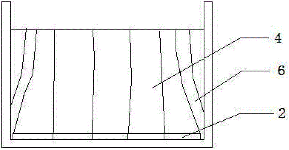
[0051] (2) Arranging molten silicon mat...

Embodiment 3

[0058] A method for preparing crystalline silicon, comprising the steps of:

[0059] (1) Randomly lay single crystal silicon seed crystals in the center of the bottom of the crucible to form a seed crystal layer. The crystal orientation of the single crystal silicon seed crystals is not limited; lay nucleation sources on the rest of the bottom to form a nucleation source layer;

[0060] Among them, the monocrystalline silicon seed crystal is a cylindrical monocrystalline silicon seed crystal with a thickness of 50 mm, a total of 1 piece, which is laid at the center of the bottom of the crucible, and the rest of the bottom is filled with nucleation sources, and the nucleation source layer is gently flattened. The thickness is about 30 mm, and the nucleation source is silicon carbide powder with a particle size of 1 cm.

[0061] (2) Arranging molten silicon material above the seed crystal layer and nucleation source layer, controlling the temperature at the bottom of the crucibl...


PUM

PropertyMeasurementUnit
thicknessaaaaaaaaaa
thicknessaaaaaaaaaa
thicknessaaaaaaaaaa

Abstract

The invention discloses a preparation method of crystalline silicon, which comprises the following steps: a mono-crystal silicon seed crystal is randomly paved in the center of the bottom of a crucible to form a seed crystal layer; a nucleation source is paved at the residual part of the bottom to form a nucleation source layer; a silicon material in a melting state is arranged on the seed crystal layer and the nucleation source layer to control the temperature of the bottom of the crucible so as to prevent the seed crystal layer and the nucleation source layer from being completely molten; and the temperature in the crucible is controlled to gradually increase to form temperature gradient in the direction vertical to the upward direction of the bottom of the crucible, so that the molten silicone material can form nuclear crystallization on the mono-crystal silicone seed crystal and the nucleation source and the crystalline silicon of which the center is mono-like and the periphery is high-effective polycrystal. The invention further discloses the crystalline silicon prepared by the preparation method for crystalline silicon. The preparation method for crystalline silicon reduces the consumption of the mono-crystal silicone seed crystal, saves the production cost, improves the quality of the silicon block in the area close to the side wall of the crucible; and monocrystal-like silicon and high-effective polycrystal silicone coexist in the prepared crystalline silicone, and the complementary advantages of the monocrystal-like silicone and the high-effective polycrystal silicone are realized.

Description

technical field [0001] The invention relates to the field of semiconductor preparation, in particular to crystalline silicon containing quasi-single crystals and high-efficiency polycrystals and a preparation method thereof. Background technique [0002] Crystalline silicon is the most commonly used semiconductor material in the manufacture of solar cells. At present, the crystalline silicon used in the manufacture of solar cells is mainly monocrystalline silicon by Czochralski method and polycrystalline silicon by ingot casting technology. Polysilicon ingot casting has large feeding capacity, simple operation, and low process cost, but the battery conversion efficiency is low and the service life is short; Czochralski monocrystalline silicon conversion efficiency is high, but single feeding is small, the operation is complicated, and the cost is high. How to combine the two into one and form complementary advantages has become a hot spot and difficulty in the development of...

Claims


Application Information

Patent Timeline
Patent Type & Authority Patents(China)
IPC IPC(8): C30B29/06C30B28/06C30B11/00
Inventor 胡动力陈红荣钟德京何亮
Owner JIANGXI SAI WEI LDK SOLAR HI TECH CO LTD
Why Eureka
Try Eureka