CMOS image sensor columns share 2×2 pixel cells and pixel arrays

An image sensor and pixel array technology, applied in image communication, electrical components, television, etc., can solve the problems of low sensitivity, amplitude (conversion gain is not large, and information is not clear enough), so as to improve light efficiency, improve image quality, Effect of increasing conversion gain

Active Publication Date: 2015-09-16
BEIJING SUPERPIX MICRO TECHNOLOGY CO LTD
View PDF4 Cites 0 Cited by
  • Summary
  • Abstract
  • Description
  • Claims
  • Application Information

AI Technical Summary

Problems solved by technology

[0005] Due to the small photosensitive area and low sensitivity of the small-area pixel sensor, the information transmitted in dark light is not clear enough
Especially when the first layer of metal, the second layer of metal and the third layer of metal are used as device interconnection lines, the dielectric height on the surface of the photodiode Si (silicon) is relatively high, and the metal lines block part of the light from entering the photodiode; Moreover, the metal line connecting the floating active area to the gate of the source follower transistor is close to the power supply metal line, and the parasitic capacitance of the floating active area is large, resulting in a small amplitude (conversion gain) for converting signal electrons into signal voltage

Method used


Image

  • CMOS image sensor columns share 2×2 pixel cells and pixel arrays
  • CMOS image sensor columns share 2×2 pixel cells and pixel arrays
  • CMOS image sensor columns share 2×2 pixel cells and pixel arrays

Examples


Embodiment 1

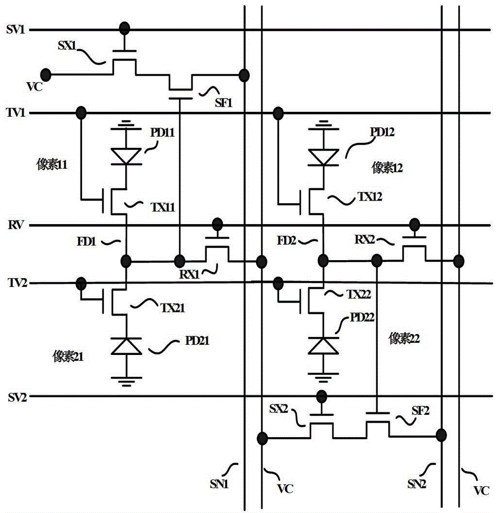
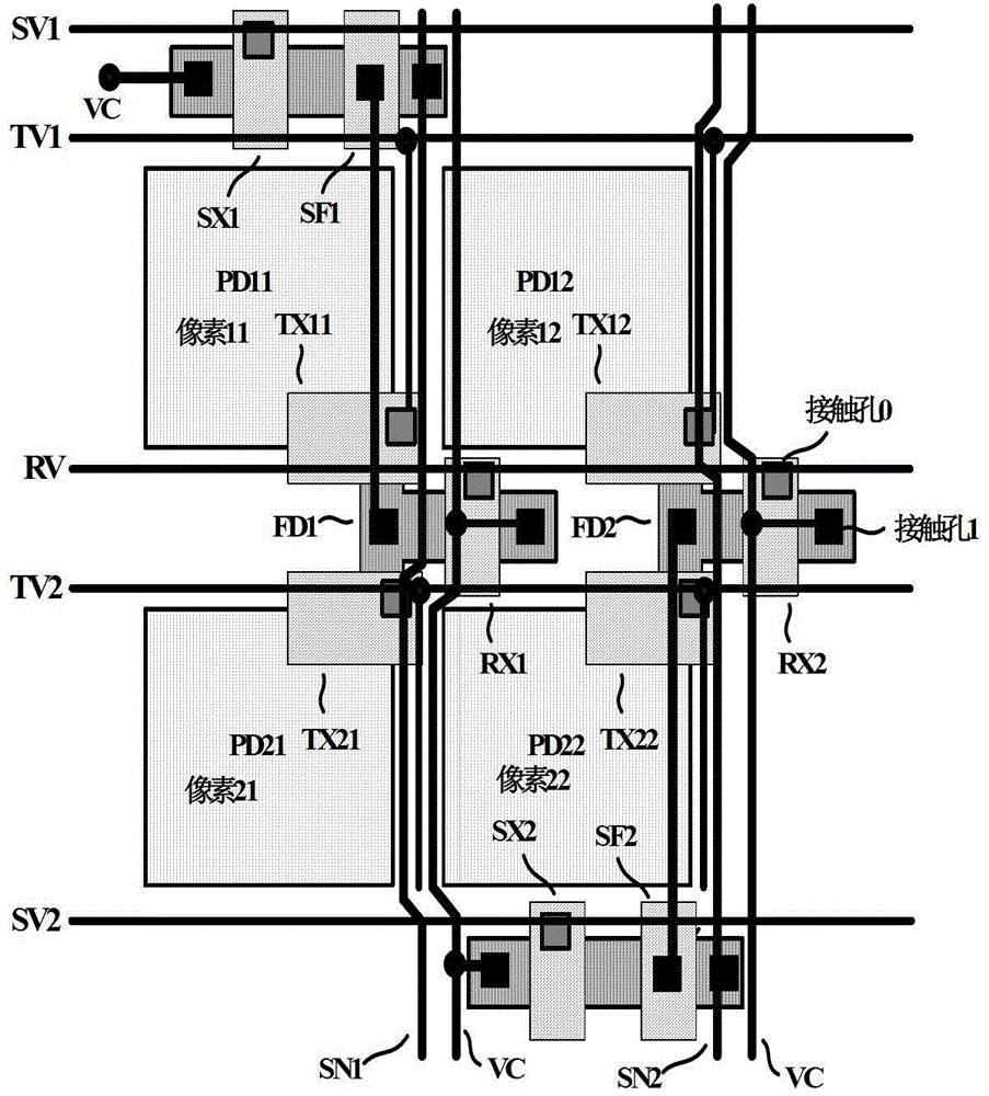
[0031] Such as figure 1 As shown in the schematic circuit diagram, the CMOS image sensor columns share 2×2 pixel units with a 4T2S structure, including four pixels, pixel 11 , pixel 12 , pixel 21 and pixel 22 . PD11, PD12, PD21 and PD22 are photodiodes of pixel 11, pixel 12, pixel 21 and pixel 22 respectively; TX11, TX12, TX21 and TX22 are charge transfer transistors of pixel 11, pixel 12, pixel 21 and pixel 22 respectively; RX1 and RX2 are reset transistors, SF1 and SF2 are source follower transistors, SX1 and SX2 are select transistors; pixel 11 and pixel 21 share reset transistor RX1, source follower transistor SF1, select transistor SX1, pixel 12 and pixel 22 share reset transistor RX2, Source follower transistor SF2 , selection transistor SX2 ; SX1 and SF1 are located on the top of pixels 11 and 21 in the front column, and SX2 and SF2 are located in the bottom of pixels 12 and 22 in the rear column. FD1 is a floating active area shared by pixel 11 and pixel 21, FD2 is a ...


PUM


Abstract

The present invention relates to a column sharing 2×2 pixel unit and a pixel array of a CMOS image sensor. Four pixels are arranged to form a 2×2 pixel array acting as a pixel unit. In each pixel unit, a front column of two pixels and a back column of two pixels each share a selection transistor, a source follower transistor, a reset transistor, and a floating active region in the column. In the two-dimensional pixel array of the CMOS image sensor, for metal connection lines, two layers of metal lines are used for connection, only a 0th layer metal line and a 1st layer metal line are used as device control lines to collect image information, but a 2nd or higher layer metal line is not used as a device control line, so that the height of the medium on the Si surface of a photodiode is decreased, and more light can enter the photodiode, so as to increase the light utilization efficiency and conversion gain of a small-area-pixel sensor, thereby increasing the sensitivity and effectively improving the image quality of the small-area-pixel image sensor.

Description

technical field [0001] The invention relates to a CMOS image sensor, in particular to a CMOS image sensor column sharing 2×2 pixel units and a pixel array. Background technique [0002] Image sensors are already widely used in digital cameras, mobile phones, medical devices, automobiles and other applications. In particular, the rapid development of CMOS (Complementary Metal Oxide Semiconductor) image sensors has made people have higher requirements for low power consumption, small size, and high resolution image sensors. [0003] The CMOS image sensor columns in the prior art share the arrangement of the 2×2 pixel unit structure. Taking 4T2S (four transistors and two pixels shared) as an example, due to the dependence on the structural characteristics of the pixels themselves, the pixel array generally requires the first layer Metal, second-level metal and third-level metal are used as device interconnection lines, and multiple rows or columns of first-level metal, second-...

Claims


Application Information

Patent Timeline
Patent Type & Authority Patents(China)
IPC IPC(8): H04N5/374H01L27/146
CPCH04N5/37457H04N25/778
Inventor 郭同辉陈杰刘志碧旷章曲唐冕
Owner BEIJING SUPERPIX MICRO TECHNOLOGY CO LTD
Why Eureka
Try Eureka