


Quick Research
Generate reliable direction feasibility study reports for your R&D in just a few steps.

Technical Q&A
Discover and master advanced knowledge NOW. Basics, ideas, possibilities, all at once.

Find Solutions
As an expert in R&D theories, this can generate solutions to your technical problems instantly.

Evaluate Feasibility
Analyze your overall solution with one click, know your potential R&D risks in advance.

Monitor Landscape
Get weekly tech updates, stay abreast of the latest tech innovations and key insights.
CMOS (complementary metal-oxide-semiconductor transistor) image sensor pixel and control time sequence thereof
An image sensor and pixel technology, used in image communication, radiation control devices, electrical solid-state devices, etc., can solve the problems of low aperture ratio of metal windows, low sensitivity, and insufficient information, so as to improve light efficiency and image quality. , the effect of improving sensitivity
- Summary
- Abstract
- Description
- Claims
- Application Information
AI Technical Summary
Problems solved by technology
Method used
Image


Examples
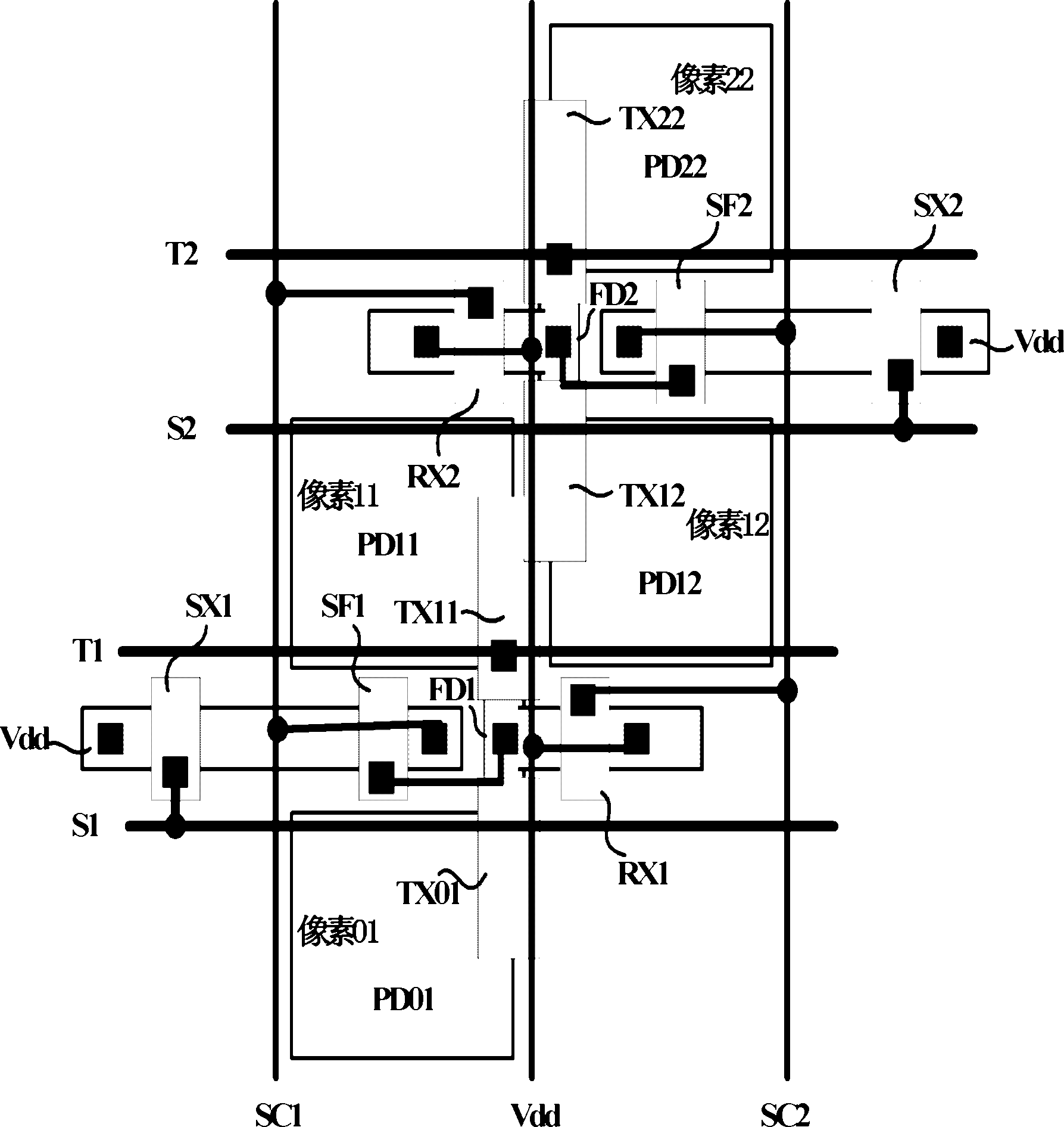
Embodiment 1
[0052] like figure 1 As shown, the CMOS image sensor pixel adopts 4T2S structure, including four pixels, the photodiodes of pixel 01, pixel 11, pixel 12 and pixel 22 are PD01, PD11, PD12, PD22 respectively; TX01 and TX11 are pixel 01 and pixel 11 respectively TX12 and TX22 are the charge transfer transistors of pixel 12 and pixel 22 respectively; SX1, SF1 and RX1 are the select transistors, source follower transistors and reset transistors of pixel 01 and pixel 11 respectively; SX2, SF2 and RX2 are respectively Select transistors, source follower transistors and reset transistors of pixels 12 and 22 . Pixel 01 and pixel 11 share transistors SX1, SF1, RX1 and floating active area FD1 (Floating Diffusion), and pixel 12 and pixel 22 share transistors SX2, SF2, RX2 and floating active area FD2; shared pixel 01 and pixel 11 and the shared pixels 12 and 22 form a mutually interlaced structure in the horizontal direction.
[0053] The metal interconnection lines used by CMOS image ...
Embodiment 2
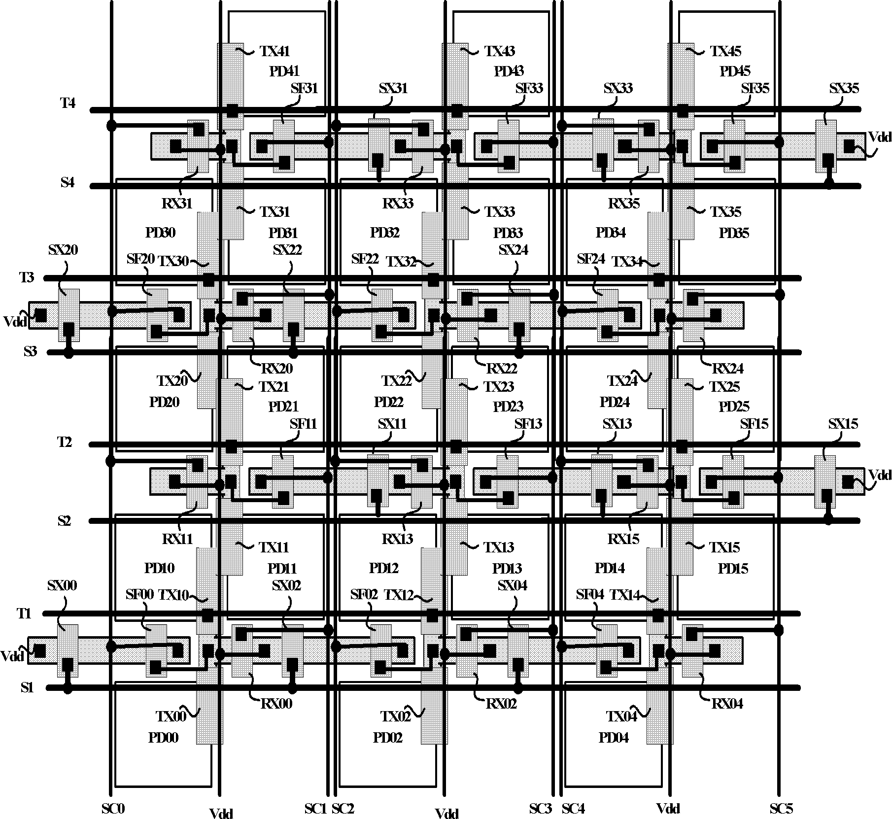
[0056] like image 3 As shown, it is a schematic diagram of a 6X4 pixel array layout; image 3 The circuit schematic diagram corresponding to the schematic diagram of the pixel array layout is as follows: Figure 4 shown.
[0057] image 3 and Figure 4 In the pixel array shown, the FD area of each pixel is connected to the gate of each corresponding source-following transistor with the first-layer metal connection, the power supply Vdd line uses the first-layer metal connection; the SC0-SC5 lines are the first-layer metal connection, The signal output line and the timing control line of the column controller are respectively connected to the source of the source follower transistor and the gate of the reset transistor of the pixel corresponding to the column. The second-layer metal connections S1 - S4 are respectively connected to the gates of the select transistors corresponding to the rows of pixels, and the second-layer metal connections T1 - T4 are respectively conn...
Embodiment 3
[0059] The details of CMOS image sensor pixel array signal acquisition are expressed as follows:
[0060] Figure 5 Shown is a schematic diagram of a pixel array with a row decoder and a column controller. The row decoder is placed on the left side of the pixel array (or on the right side of the array), the column controller is placed on the top of the pixel array (or on the bottom of the array), and the signal readout device is placed on the side of the pixel array. Bottom: The positions of the decoder, controller and signal readout device are not the only method of the present invention, and can also be adjusted according to the specific design and layout of the chip. Figure 5 In the schematic diagram shown, the specific positions of the array pixels are marked in detail, and the specific numbers of the timing output control lines of the decoder and the timing control lines of the column controller are also marked in detail. m and n are non-negative integers, which repres...
PUM
 Abstract
Description
Claims
Application Information
 - R&D Engineer
- R&D Manager
- IP Professional
- Industry Leading Data Capabilities
- Powerful AI technology
- Patent DNA Extraction
Browse by: Latest US Patents, China's latest patents, Technical Efficacy Thesaurus, Application Domain, Technology Topic, Popular Technical Reports.
© 2024 PatSnap. All rights reserved.Legal|Privacy policy|Modern Slavery Act Transparency Statement|Sitemap|About US| Contact US: help@patsnap.com