


Quick Research
Generate reliable direction feasibility study reports for your R&D in just a few steps.

Technical Q&A
Discover and master advanced knowledge NOW. Basics, ideas, possibilities, all at once.

Find Solutions
As an expert in R&D theories, this can generate solutions to your technical problems instantly.

Evaluate Feasibility
Analyze your overall solution with one click, know your potential R&D risks in advance.

Monitor Landscape
Get weekly tech updates, stay abreast of the latest tech innovations and key insights.
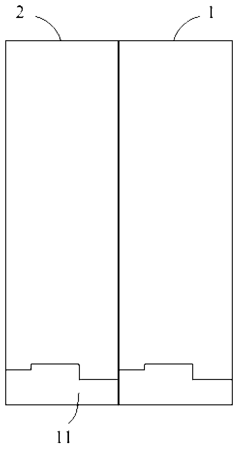
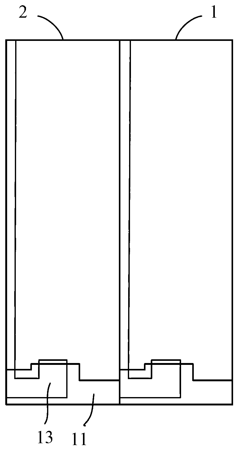
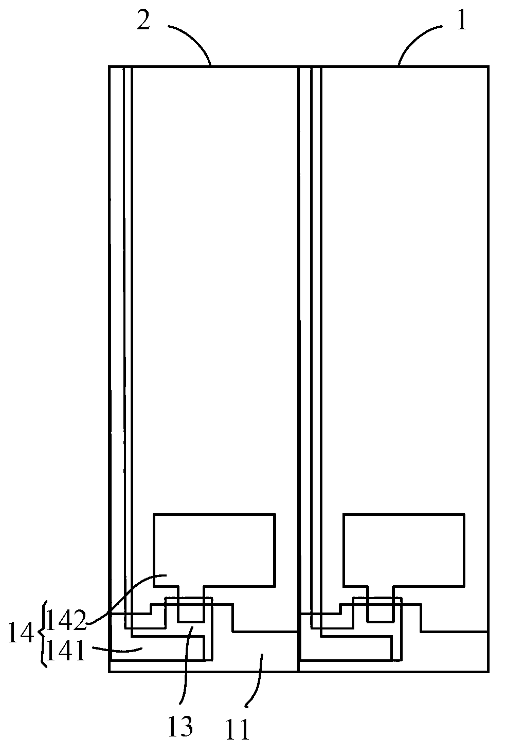
Pixel structure of display panel and manufacturing method thereof
A technology of pixel structure and manufacturing method, used in static indicators, nonlinear optics, instruments, etc., can solve the problems of short circuit, the pixel aperture ratio cannot be effectively improved, and the panel cannot display images normally, and achieves the improvement of the pixel aperture ratio. Effect
- Summary
- Abstract
- Description
- Claims
- Application Information
AI Technical Summary
Problems solved by technology
Method used
Image

Examples
Embodiment Construction
[0032] The present invention relates to a pixel structure of a display panel and a manufacturing method thereof, which is characterized in that the pixel electrodes in two adjacent pixel areas are arranged at different levels. It can also be said that the two pixel electrodes are formed at different heights. layer, whereby the horizontal spacing between the pixel electrodes in two adjacent pixel areas can be reduced compared to the spacing specified in the manufacturing process, that is to say, the area occupied by the pixel electrodes is relatively larger, so the present invention can effectively Increase opening rate. On the other hand, in the present invention, a conductive layer (or metal conductive layer) can be arranged at the junction of two adjacent pixel areas, and the conductive layer can respectively form a storage capacitor with the pixel electrodes in the two adjacent pixel areas, and the conductive layer can also The coupling effect of two adjacent pixel electrod...
PUM
 Abstract
Description
Claims
Application Information
 - R&D Engineer
- R&D Manager
- IP Professional
- Industry Leading Data Capabilities
- Powerful AI technology
- Patent DNA Extraction
Browse by: Latest US Patents, China's latest patents, Technical Efficacy Thesaurus, Application Domain, Technology Topic, Popular Technical Reports.
© 2024 PatSnap. All rights reserved.Legal|Privacy policy|Modern Slavery Act Transparency Statement|Sitemap|About US| Contact US: help@patsnap.com