
Full-angle luminous LED (light-emitting diode) chip encapsulation structure

A LED chip, full-angle light-emitting technology, applied to electrical components, circuits, semiconductor devices, etc., can solve the problems of LED luminous brightness loss, low LED chip power, and no package structure for full-angle light, and the structure is easy to realize Effect

Inactive Publication Date: 2013-01-02
SUZHOU JINKE XINHUI PHOTOELECTRIC TECH
View PDF5 Cites 6 Cited by
  • Summary
  • Abstract
  • Description
  • Claims
  • Application Information

AI Technical Summary

Problems solved by technology

[0003] Due to the low power of the previous LED chip, the existing packaging structure reflects and converges the light into a beam of unidirectional light to increase the luminous intensity in a certain direction, but this method will cause light absorption and shading, causing the LED to emit light. loss of brightness
Now with the development of technology, the power of LED chips has been greatly increased, which can realize full-angle light emission, but there is no package structure that can realize full-angle light emission.

Method used


Image

  • Full-angle luminous LED (light-emitting diode) chip encapsulation structure

Examples


Embodiment Construction

[0014] The present invention will be specifically introduced below in conjunction with the accompanying drawings and specific embodiments.

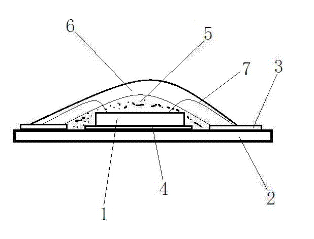
[0015] Such as figure 1 As shown, the packaging structure of an all-angle light-emitting LED chip mainly includes: an LED chip 1 , a substrate 2 , an electrode 3 , a first adhesive layer 4 , a second adhesive layer 5 , and a protective adhesive layer 6 .

[0016] Wherein, the substrate 2 is used as a carrier for carrying the LED chip 1, and the LED chip 1 is arranged on the front of the substrate 2, and the corresponding front of the substrate 2 may also be provided with some circuits or other structures for mounting the LED chip. As a preferred solution, the base material 2 is a sheet made of a transparent resin material, specifically, the base material 2 is made of a transparent PET or PC material. The substrate 2 of the sheet is convenient for fixing the LED chips 1 . A first adhesive layer 4 is provided between the LED chip 1 and th...


PUM


Abstract

The invention discloses a full-angle luminous LED (light-emitting diode) chip encapsulation structure, which comprises an LED chip. The full-angle luminous LED chip encapsulation structure is characterized by further comprising a base material, an electrode, a first adhesive layer, a second adhesive layer and a protective adhesive layer, wherein the base material is used for bearing the LED chip on the front side; the electrode is arranged on the front side of the base material and is used for being electrically connected with the outside; the first adhesive layer is arranged between the base material and the LED chip; the second adhesive layer is used for covering the LED chip; the protective adhesive layer is coated at the outer side of the second adhesive layer for playing a protection role; the LED chip is completely cladded by the first adhesive layer and the second adhesive layer; the first adhesive layer, the second adhesive layer and the protective adhesive layer are transparent; and the electrode and the LED chip are electrically connected. The full-angle luminous LED chip encapsulation structure has the beneficial effects that full-angle lightening of the LED can be achieved, and meanwhile, the full-angle luminous LED chip encapsulation structure is simple in structure and can fully protect the LED chip, and the machining technology is easy to realize.

Description

technical field [0001] The invention relates to a package structure of an LED chip, in particular to a package structure of an all-angle light-emitting LED chip. Background technique [0002] LED light-emitting diodes have been recognized as the most efficient artificial lighting technology in the world. Today, LED lighting is widely used in various indicator lights, street lights, holiday lights, notebooks, and TV backlights. Due to their high energy efficiency, it is widely believed that replacing traditional light bulbs, fluorescent lamps with LED lights is a very environmentally friendly practice. [0003] Due to the low power of the previous LED chip, the existing packaging structure reflects and converges the light into a beam of unidirectional light to increase the luminous intensity in a certain direction, but this method will cause light absorption and shading, causing the LED to emit light. loss of brightness. Now with the development of technology, the power of ...

Claims


Application Information

Patent Timeline
Patent Type & Authority Applications(China)
IPC IPC(8): H01L33/48H01L33/54
Inventor 傅立铭
Owner SUZHOU JINKE XINHUI PHOTOELECTRIC TECH
Learn More