


Quick Research
Generate reliable direction feasibility study reports for your R&D in just a few steps.

Technical Q&A
Discover and master advanced knowledge NOW. Basics, ideas, possibilities, all at once.

Find Solutions
As an expert in R&D theories, this can generate solutions to your technical problems instantly.

Evaluate Feasibility
Analyze your overall solution with one click, know your potential R&D risks in advance.

Monitor Landscape
Get weekly tech updates, stay abreast of the latest tech innovations and key insights.
A kind of manufacturing method of led filament
A technology of LED filament and manufacturing method, which is applied in the direction of electrical components, electric solid devices, circuits, etc., which can solve the problems of uneven light output, high cost, and low benefit, and achieve the effects of uniform light color, low cost, and small equipment investment
- Summary
- Abstract
- Description
- Claims
- Application Information
AI Technical Summary
Problems solved by technology
Method used
Image

Examples
Embodiment 1
[0033] A method for manufacturing an LED filament in this embodiment specifically includes the following steps:
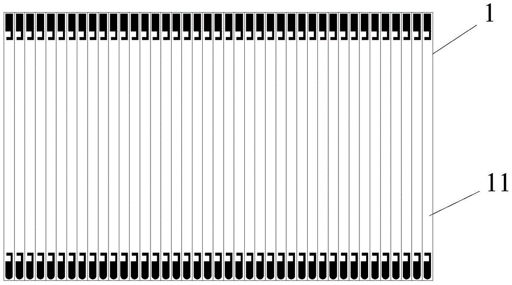
[0034] 1) if figure 1 As shown, print pads on the entire base, and pre-split each base 1, and use a laser cutting machine to cut the base to ensure that each base 1 has a half-cut state;
[0035] Wherein, the base 1 can be made of glass, ceramic or metal material, in this embodiment, the base is preferably glass;
[0036] Wherein, the base 1 is a columnar body with a rectangular parallelepiped structure, and the ratio between the length and width is 15-40. Preferably, the width range is 0.8-1.2 mm, the length range is 20-40 mm, and the height range is 0.2-0.8 mm. ;
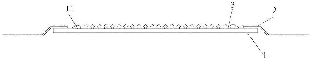
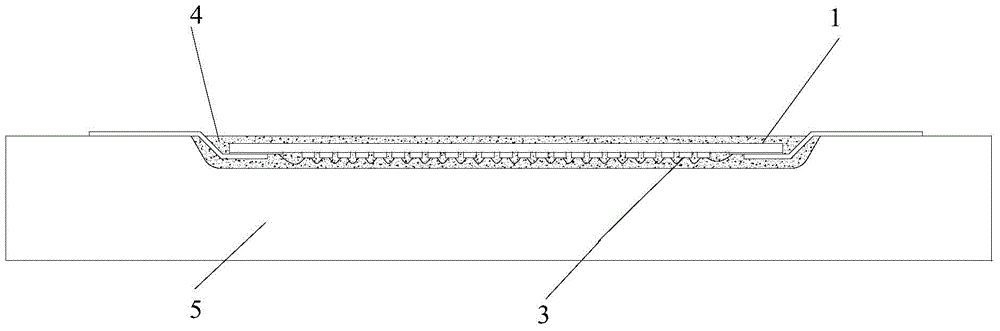
[0037] Wherein, the base 1 has at least one LED chip mounting surface, in this embodiment, the base has one LED chip mounting surface 11;
[0038] 2) LED chips are placed on the chip mounting surface of the base, and there are multiple LED chips on each base, and these LED chips are connected in ser...
Embodiment 2
[0050] The main difference between the LED filament manufacturing method provided in this embodiment and the LED filament manufacturing method provided in Embodiment 1 is:
[0051] The base provided by Embodiment 1 has an LED chip mounting surface, and the base of this embodiment is as Figure 4 As shown, there are two LED chip mounting surfaces, respectively the first LED chip mounting surface 11 and the second LED chip mounting surface 12, the first LED chip mounting surface 11 is arranged along the horizontal direction, and the second LED chip mounting surface 12 is parallel to The first LED chip mounting surface 11, in other embodiments, the second LED chip mounting surface 12 can also intersect with the first LED chip mounting surface 11, each LED chip mounting surface is provided with a The bent electrode 2 electrically connected to the disk, the structure of the bent electrode 2 is the same as that of the bent electrode in the first embodiment, and will not be repeated ...
Embodiment 3
[0053] The main difference between the LED filament manufacturing method provided in this embodiment and the LED filament manufacturing method provided in Embodiment 1 is:
[0054] The base provided in Embodiment 1 has an LED chip mounting surface, and the base 1 of this embodiment is as Figure 5 , 6 As shown, there are four LED chip mounting surfaces, which are respectively the first LED chip mounting surface 11, the second LED chip mounting surface 12, the third LED chip mounting surface 13 and the fourth LED chip mounting surface 14. The first LED chip mounting surface The surface 11 is arranged along the horizontal direction, the second LED chip 12 mounting surface is parallel to the first LED chip mounting surface, the third LED chip mounting surface 13 and the fourth LED chip mounting surface 14 are respectively located on both sides of the first LED chip mounting surface, Each chip mounting surface is provided with a bent electrode 2 that is electrically connected to ...
PUM
 Abstract
Description
Claims
Application Information
 - R&D Engineer
- R&D Manager
- IP Professional
- Industry Leading Data Capabilities
- Powerful AI technology
- Patent DNA Extraction
Browse by: Latest US Patents, China's latest patents, Technical Efficacy Thesaurus, Application Domain, Technology Topic, Popular Technical Reports.
© 2024 PatSnap. All rights reserved.Legal|Privacy policy|Modern Slavery Act Transparency Statement|Sitemap|About US| Contact US: help@patsnap.com