Chip packaging method and wafer manufactured through chip packaging method

A chip packaging and wafer technology, used in semiconductor/solid-state device manufacturing, printing devices, printing, etc., can solve problems such as chip overflow, and achieve the effect of avoiding wafer warpage and avoiding the separation of adhesive and chip.

Inactive Publication Date: 2012-12-26
DIODES SHANGHAI +2
View PDF4 Cites 5 Cited by
  • Summary
  • Abstract
  • Description
  • Claims
  • Application Information

AI Technical Summary

Problems solved by technology

[0010] see Figure 3A As shown, the wafer contains chips 301, 302, and 303, and the adhesive layer 31 is formed on the back of the chips 301, 302, and 303 by applying paste adhesive on the back of the wafer. Adhesive applied on the backside, resulting in overflow at the edge of the chip

Method used


Image

  • Chip packaging method and wafer manufactured through chip packaging method
  • Chip packaging method and wafer manufactured through chip packaging method
  • Chip packaging method and wafer manufactured through chip packaging method

Examples


Embodiment Construction

[0032] The specific implementation of the chip packaging method provided by the present invention will be described in detail below in conjunction with the accompanying drawings.

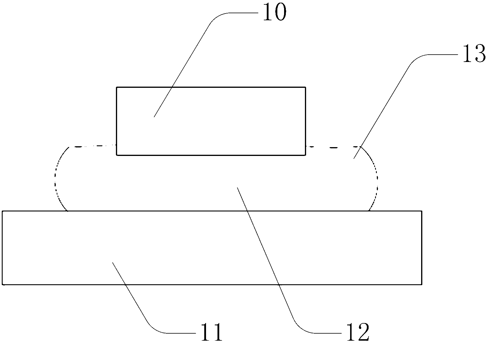
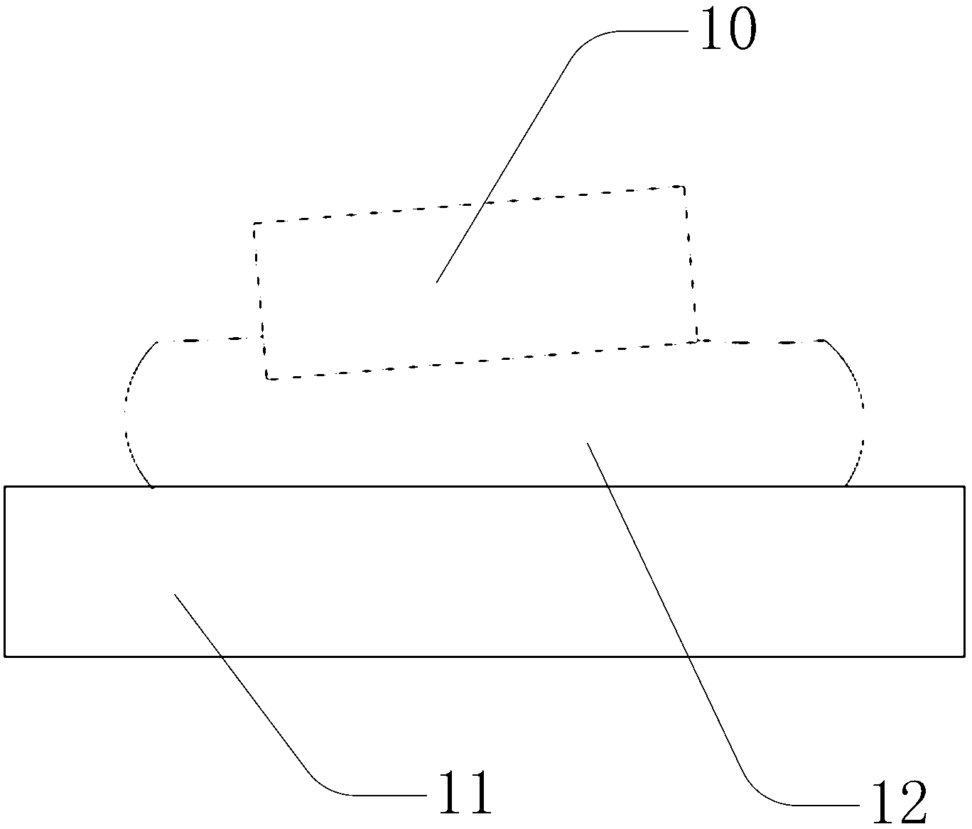
[0033] Figure 4 A schematic diagram of the steps of the chip packaging method of the present invention is shown. see Figure 4 , the chip packaging method includes the following steps: step S40, providing a wafer, the front of the wafer has a plurality of chips; S41, printing a chip adhesive on the back of each chip of the wafer with a screen, the screen has Multiple holes, each corresponding to a chip position; S42, dicing the wafer into multiple individual chips, each chip has an adhesive on the back; S43, providing a lead frame, and passing the chip through the bonding on the back paste on the lead frame; S44, wire bonding; S45, plastic packaging.

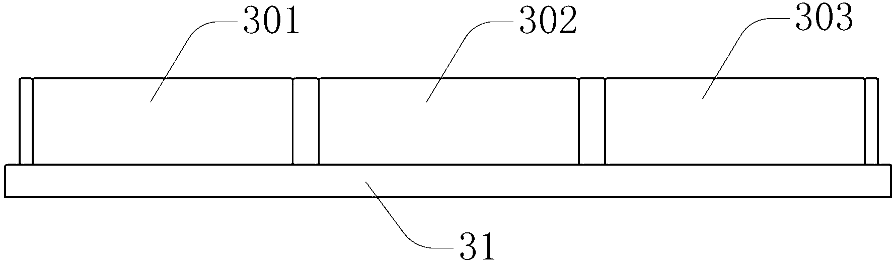
[0034] Figure 5A Shown is a schematic diagram of the wafer structure used in the present invention, and a plurality of chips 501 are distribute...


PUM


Abstract

The invention provides a chip packaging method and a wafer manufactured through the chip packaging method. The method is used in the semi-conductor technology packaging field. The chip packaging method comprises the following steps: (1) providing a wafer, (2) brushing chip adhesion agents on the back of each chip of the wafer through a silk screen, (3) cutting the wafer into a plurality of independent chips, (4) providing a leading wire frame and pasting each chip on the leading wire frame through the adhesion agents on the back of each chip. The front of the wafer is provided with a plurality of the chips. The silk screen is provided with a plurality of holes and each hole corresponds to a position of each chip. The back of each chip is provided with the adhesion agent. As each chip of the wafer is individually brushed with the adhesion agents, the chip packaging method avoids warping of the wafer caused by inner stress of the adhesion agents and overcomes the problem that the adhesion agents and the chips are separated during cutting.

Description

technical field [0001] The invention relates to the technical field of semiconductor device packaging, in particular to a chip packaging method and a wafer manufactured by the method. Background technique [0002] In the semiconductor industry, the purpose of chip packaging is to protect the bare chip from moisture, heat and noise, and to provide a medium for electrical connection between the bare chip and external circuits, such as printed circuit boards or other packaging substrates. In the packaging process, the chip needs to be fixed on the lead frame, and the chip is generally fixed on the lead frame by adhesive bonding. [0003] Currently, the traditional die-attach technology of paste die-attach dispensed through a syringe needle is gradually showing its limitations in the ever-changing semiconductor packaging industry. [0004] First, there is the issue of the speed at which the adhesive is dispensed. In some cases, the speed of adhesive dispensing becomes increasi...

Claims


Application Information

Patent Timeline
IPC IPC(8): H01L21/50H01L23/00B41M1/12
CPCH01L24/27H01L24/29H01L24/83H01L2224/83191H01L2924/01322H01L2924/12041H01L2924/00
Inventor WU TENGFEIJIANG MINJIGAO HONGTAO
Owner DIODES SHANGHAI
Why Eureka
Try Eureka