Memory structure of 3D NAND memory and method for manufacturing the same

A memory structure and memory technology, which is applied in the field of memory, can solve the problems of large degree of wafer warpage, uneven stress distribution, and reduced registration accuracy, and achieve the effects of avoiding wafer warpage and simple preparation methods

Inactive Publication Date: 2017-11-17
YANGTZE MEMORY TECH CO LTD
View PDF6 Cites 6 Cited by
  • Summary
  • Abstract
  • Description
  • Claims
  • Application Information

AI Technical Summary

Problems solved by technology

As the number of 3D NAND stacks increases, the stress distribution caused by the multi-layer film stack is uneven, which makes the warpage of the wafer more and more serious during the manufacturing process.
As a result, the alignment accuracy when etching to form vertical connection channels is greatly reduced, and the vertical connection channels often cannot be accurately connected to the stepped metal gate layer one by one, and ultimately cannot form an effective storage word line area.

Method used


Image

  • Memory structure of 3D NAND memory and method for manufacturing the same
  • Memory structure of 3D NAND memory and method for manufacturing the same
  • Memory structure of 3D NAND memory and method for manufacturing the same

Examples


Embodiment Construction

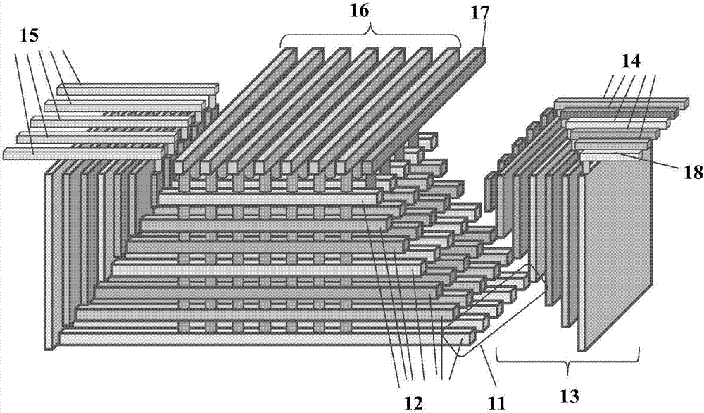
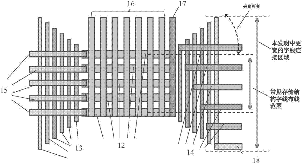
[0047] In order to avoid the phenomenon that the vertical connection channels formed due to wafer warpage cannot be accurately connected with the stepped metal gate layer one by one, and thus cannot form an effective storage word line area, the application provides an integrated method of the stepped metal gate layer and the vertical connection channel. The storage structure of the formed 3D NAND memory and its preparation method. Since the metal gate and the vertical conduction layer are integrally formed, the storage structure and its preparation method can ensure that the vertical conduction layer is connected with the stepped metal gate layer one by one accurately, thereby forming an effective storage word line region.

[0048] In addition, in the embodiment of the present application, the stepped shape of the metal gate layer in the storage structure can be automatically formed during the process of film deposition. Therefore, the preparation method provided in this embodi...


PUM


Abstract

The embodiment of the application provides a memory structure of a 3D NAND memory and a method for manufacturing the same. According to the preparation method, metal gates and vertical conducting layers are integrated into one; all gate bars on the same metal gate layer are connected with one same vertical conducting layer and the metal gates are in conduction with word lines, so that the influence of wafer warping during a vertical connection channel manufacturing process in the prior art is eliminated. Moreover, the metal gates and the vertical conducting layers are integrated, so that the vertical conducting layers are connected accurately with the stepped metal gate layers one by one and thus an effective work line storage region is formed.

Description

technical field [0001] The present application relates to the technical field of memory, in particular to a storage structure of a 3D NAND memory and a preparation method thereof. Background technique [0002] 3D NAND memory is a flash memory device with a three-dimensional stack structure, and its storage core area is composed of alternately stacked metal gate layers and insulating layers combined with vertical channel transistors. Under the condition of the same area, the more metal gate layers stacked vertically, the higher the storage density and capacity of the flash memory device. At present, the number of metal gate stack layers in common storage structures can reach tens to hundreds of layers. [0003] The stacked metal gate layers in a common 3D NAND memory have a stepped shape, and each stepped surface is independently connected to a vertical metal connection to form a storage word-line (Word-line) area. The storage structure with such a stepped shape is usually ...

Claims


Application Information

Patent Timeline
IPC IPC(8): H01L27/11582H01L27/1157H01L27/11556H01L27/11524
CPCH10B41/35H10B41/27H10B43/35H10B43/27
Inventor 陈子琪吴关平张高升
Owner YANGTZE MEMORY TECH CO LTD
Why Eureka
Try Eureka