Touch display panel and preparation method thereof as well as display device

A touch display panel and control line technology, applied in the direction of static indicators, instruments, electrical digital data processing, etc., can solve the problems of common electrode voltage instability, noise, touch accuracy, etc., to improve touch accuracy and accuracy sexual effect

Inactive Publication Date: 2012-12-19
BOE TECH GRP CO LTD +1
View PDF6 Cites 9 Cited by
  • Summary
  • Abstract
  • Description
  • Claims
  • Application Information

AI Technical Summary

Problems solved by technology

[0003] In the prior art, optical touch sensing generally uses an optical sensing thin film transistor (optical sensing TFT) to sense light intensity, and the gate and source of the optical sensing TFT are connected to the common electrode lines on the array substrate , because the voltage of the common electrode is limited by the array substrate, it cannot be adjusted arbitrarily; and the common electrode will be interfered by the data signal line during actual work, resulting in certain noise, so the voltage of the common electrode is not maintained at the actual working process A constant DC voltage, which will have a certain impact on the touch accuracy and judgment accuracy
At the same time, since the optical sensing TFT is connected to the common electrode line, it will affect the stability of the voltage on the common electrode line, which will cause the voltage on the common electrode to be unstable, thereby affecting the display of the pixel.

Method used


Image

  • Touch display panel and preparation method thereof as well as display device
  • Touch display panel and preparation method thereof as well as display device
  • Touch display panel and preparation method thereof as well as display device

Examples


Embodiment Construction

[0030] In order to make the technical problems, technical solutions and advantages to be solved by the embodiments of the present invention clearer, the following will describe in detail with reference to the drawings and specific embodiments.

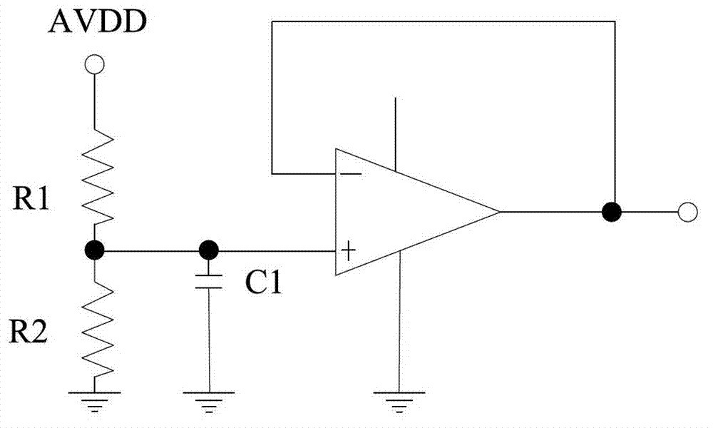
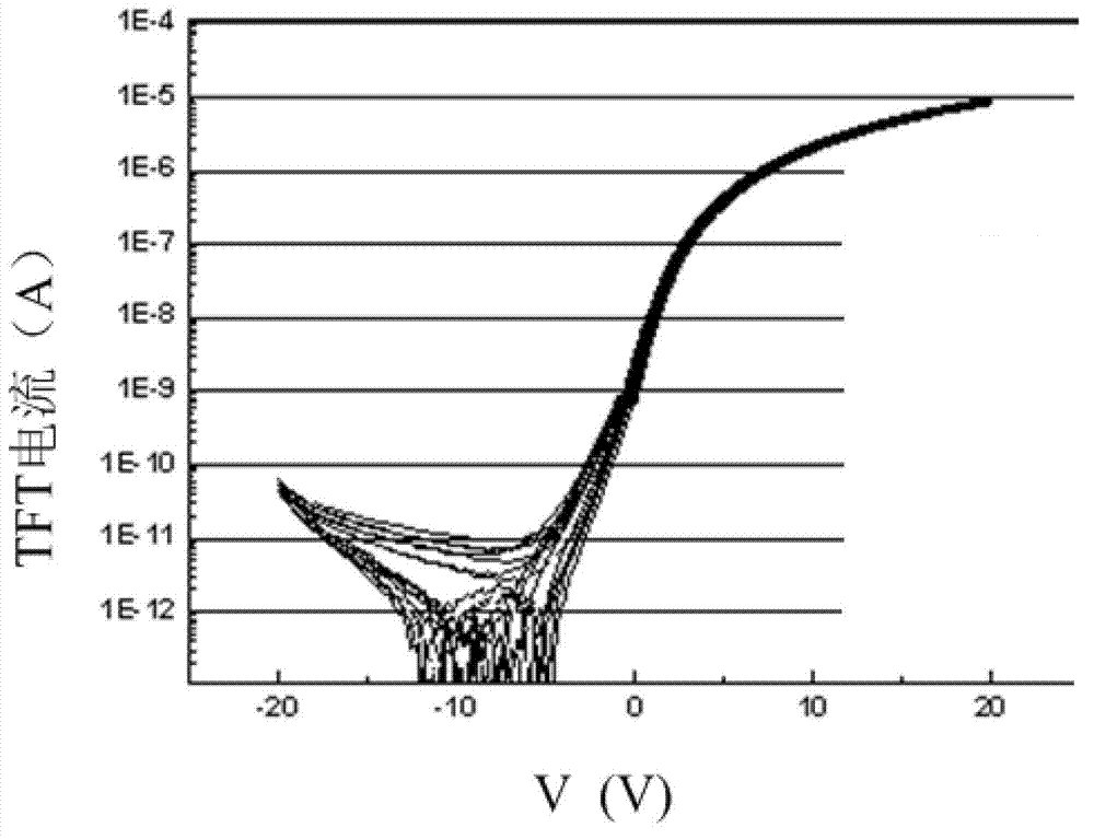
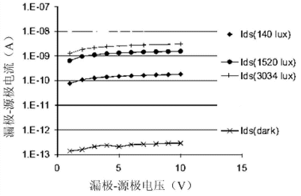
[0031] In the embodiment of the present invention, both the gate and the source of the optical sensing TFT are connected to the common electrode line of the array substrate. At this time, the stability of the voltage on the common electrode line will be affected, resulting in the voltage on the common electrode Unstable, affecting the display effect of pixels. The invention provides a touch display panel which does not affect the voltage of a common electrode, a preparation method thereof, and a display device.

[0032] The touch display panel according to the embodiment of the present invention includes an array substrate on which a plurality of gate lines and a plurality of common electrode lines are arranged, and the touch display p...


PUM


Abstract

The invention provides a touch display panel and a preparation method thereof as well as a display device, belonging to the field of a touch screen display. The touch display panel comprises an array substrate and the array substrate is provided with a plurality of grid wires and a plurality of public electrode wires; the touch display panel further comprises a plurality of optical sensing units arranged on the array substrate, an optical sensing control wire arranged on the array substrate, an optical sensing signal wire arranged on the array substrate and a voltage supply unit, wherein each optical sensing unit comprises an optical sensing TFT (Thin Film Transistor); a grid electrode and a drain electrode of the optical sensing TFT are connected with the optical sensing control wire; the optical sensing signal wire is crossly arranged with the optical sensing control wire; one end of the optical sensing signal wire is connected with the optical sensing units and is used for outputting an optical sensing signal; and the voltage supply unit is used for providing stable voltage to the optical sensing TFT through the optical sensing control wire. The technical scheme disclosed by the invention can improve touch precision and accuracy.

Description

technical field [0001] The invention relates to the field of touch screen displays, in particular to a touch display panel, a manufacturing method thereof, and a display device. Background technique [0002] According to the principle, the touch screen generally includes the following types: resistive touch screen, capacitive touch screen, infrared touch screen, surface acoustic wave touch screen, electromagnetic touch screen, vibration induction touch screen, frustrated total internal reflection optical induction, etc. According to the composition structure, the touch screen is divided into: external touch screen (double layer), touch sensor on the coverage surface (single layer), touch sensor on the panel, and touch sensor inside the panel. With the market development trend of overall module thinning, the structure of the touch screen is developed from an external touch screen to an embedded touch screen, which can not only reduce the thickness of the touch panel but also ...

Claims


Application Information

Patent Timeline
Patent Type & Authority Applications(China)
IPC IPC(8): G06F3/042G02F1/133
Inventor 徐宇博胡明林炳仟
Owner BOE TECH GRP CO LTD
Why Eureka
Try Eureka