
Manufacturing method for heavy-copper printed circuit boards

A technology for printed circuit boards and manufacturing methods, which is applied in the direction of printed circuits, printed circuit manufacturing, and electrical components, and can solve the problems of low reliability of HASL, explosion of boards, and reduction of HASL costs, so as to reduce the amount of tin used , cost reduction and yield improvement

Active Publication Date: 2012-12-12
WUS PRINTED CIRCUIT (KUNSHAN) CO LTD
View PDF4 Cites 17 Cited by
  • Summary
  • Abstract
  • Description
  • Claims
  • Application Information

AI Technical Summary

Problems solved by technology

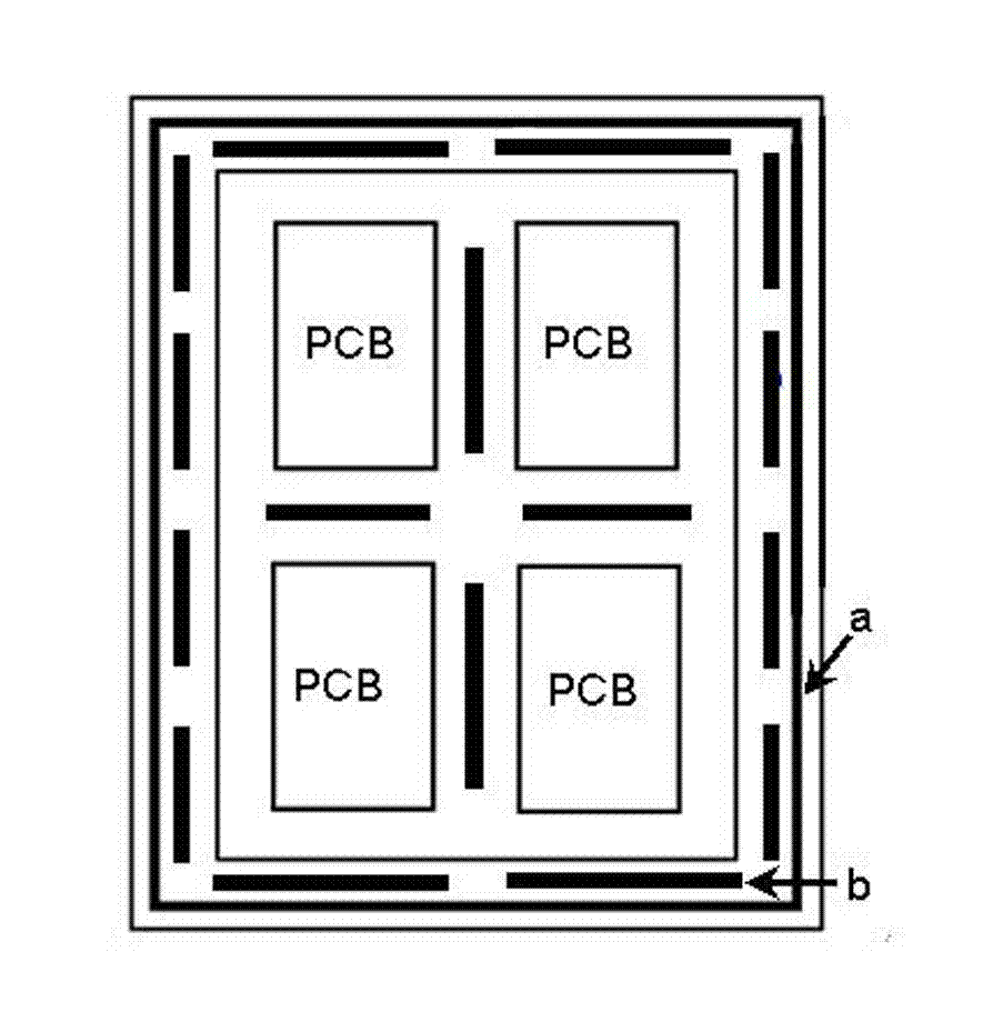
[0003] In order to solve the board explosion problem caused by the stress generated by the high temperature in the process of tinning the thick copper plate, the present invention mills off the frame of the circuit board before the tinning process and mills a certain number of hollow areas between the non-effective graphic areas on the edge of the board or between the typesetting spacing. Relieve thermal stress, overcome the risk of low reliability of HASL, and solve the problem of cracking boards. HASL can also reduce the amount of tin used after milling off the frame, further reducing the cost of HASL

Method used


Image

  • Manufacturing method for heavy-copper printed circuit boards
  • Manufacturing method for heavy-copper printed circuit boards
  • Manufacturing method for heavy-copper printed circuit boards

Examples


Embodiment Construction

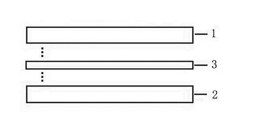
[0032] In order to further reveal the technical solutions of the present invention, the following describes the implementation of the present invention in detail in conjunction with the accompanying drawings: figure 2 As shown, a thick copper printed circuit board includes at least two inner substrates, that is, a first inner substrate 1 and a second inner substrate 2, and an adhesive sheet 3 is arranged between the two inner substrates. Such as image 3 As shown, there is a hollow area b between the non-effective graphic area or the typesetting spacing on the edge of the board.

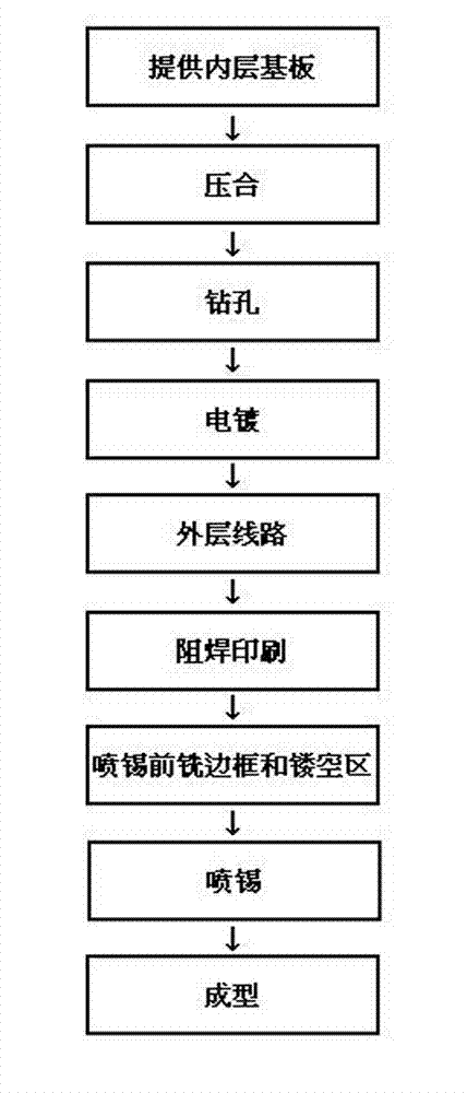
[0033] Such as Figure 1 to Figure 3 Shown, a kind of manufacturing method of thick copper type printed circuit board comprises the following steps:

[0034] (1) Provide inner substrates: First, provide at least two inner substrates as required, namely the first inner substrate 1 and the second inner substrate 2, at least one inner substrate with a copper thickness ≥ 3oz, in each inner substrate ...


PUM


Abstract

The invention discloses a manufacturing method for heavy-copper printed circuit boards. The manufacturing method includes steps of (1), providing an inner substrate; (2), pressing and fitting; (3) boring; (4) electroplating; (5), manufacturing outer circuits; (6), printing solder masks; (7), milling frames and hollow-out areas before spraying solders; (8) spraying the solders; and (9) molding. By the manufacturing method, problems such as poor quality and waste of time, manpower and material resources due to high temperature during solder spraying are solved, and board delamination during solder spraying in manufacturing of the heavy-copper printed circuit boards is overcome. In addition, by the manufacturing method which is simple and feasible, the yield of the solder spraying (especially lead-free solder spraying) process for heavy-copper boards can be improved greatly and production cost can be reduced further.

Description

technical field [0001] The invention relates to a method for manufacturing a printed circuit board, in particular to a method for manufacturing a thick copper printed circuit board, which belongs to the field of printed circuit board manufacturing. Background technique [0002] At present, this kind of thick copper printed circuit board is usually baked and heated first when spraying tin, so that the temperature of the board surface is raised appropriately, and then pretreatment before tin spraying, fluxing, and tin spraying are performed. The disadvantages of this method are : After HASL (especially lead-free HATS), the risk of reliability is high, and it is easy to have the problem of board explosion. Contents of the invention [0003] In order to solve the board explosion problem caused by the stress generated by the high temperature in the process of tinning the thick copper plate, the present invention mills off the frame of the circuit board before the tinning proces...

Claims


Application Information

Patent Timeline
Patent Type & Authority Applications(China)
IPC IPC(8): H05K3/00
Inventor 徐友福胡赵霞
Owner WUS PRINTED CIRCUIT (KUNSHAN) CO LTD
Learn More