Packaging structure for active matrix organic electroluminescent diode panel

A packaging structure and matrix technology, applied in circuits, electrical components, electric solid devices, etc., can solve the problems of poor adhesion and inability to achieve, achieve excellent sealing and adhesion of packaging, and solve poor adhesion. Effect

Inactive Publication Date: 2012-11-21
TCL CHINA STAR OPTOELECTRONICS TECH CO LTD
View PDF5 Cites 1 Cited by
  • Summary
  • Abstract
  • Description
  • Claims
  • Application Information

AI Technical Summary

Problems solved by technology

[0007] 5. Good low-temperature characteristics, it can still display normally at minus 40 degrees, but LCD can't do it;
However, because the material of glass glue is hard, although it can effectively block water and oxygen, its adhesion is not good. Therefore, if you want to realize a large-scale active matrix OLED panel, the adhesion between the substrate and the back cover is very important. Glass glue will be a severe test, so the packaging of large-size active matrix OLED panels needs to take into account the adhesion and the ability to block water and oxygen

Method used


Image

  • Packaging structure for active matrix organic electroluminescent diode panel
  • Packaging structure for active matrix organic electroluminescent diode panel
  • Packaging structure for active matrix organic electroluminescent diode panel

Examples


Embodiment Construction

[0030] In order to further illustrate the technical means adopted by the present invention and its effects, the following describes in detail in conjunction with preferred embodiments of the present invention and accompanying drawings.

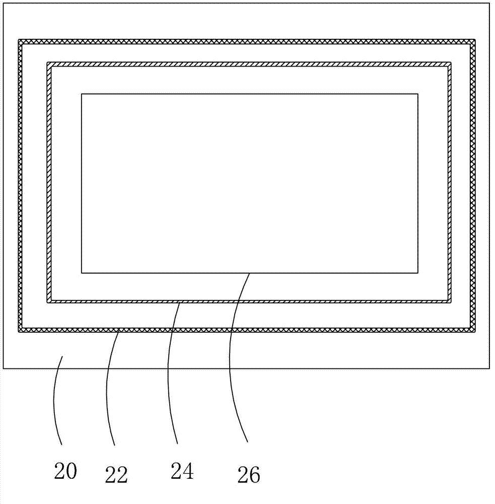
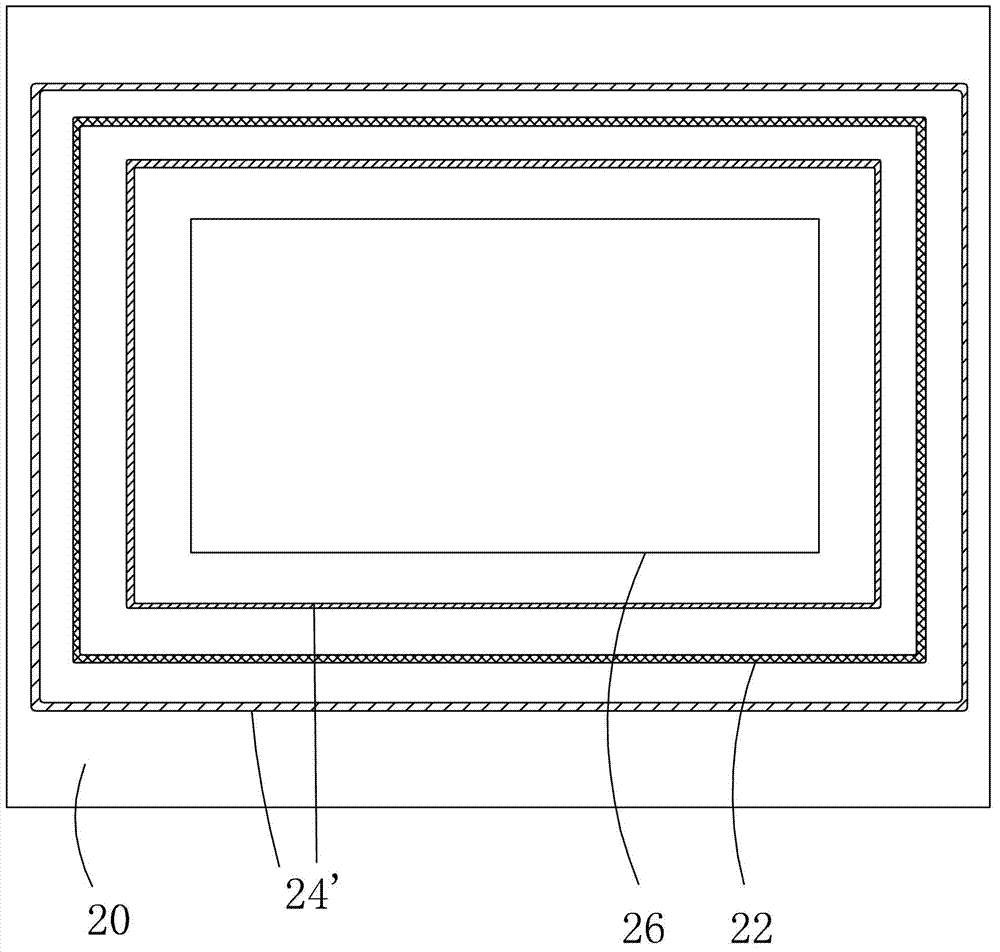
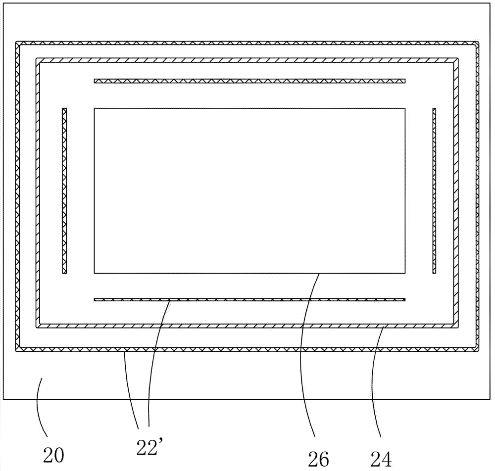
[0031] see figure 1 , the present invention provides a packaging structure of an active matrix organic electroluminescent diode panel, comprising: a substrate 20, a pixel region 26 located on the substrate 20, several turns of inorganic Packaging material 24, several turns of organic bonding material 22 located outside the pixel area 26 on the substrate 20, and a back cover (not shown) covering the inorganic packaging material 24 and the organic bonding material 22, the several turns of inorganic packaging material 24 At least one circle of the organic adhesive material 22 airtightly surrounds the pixel area 26 , at least one circle of the organic adhesive material 22 airtightly surrounds the pixel area 26 , and the inorganic packaging materia...


PUM

PropertyMeasurementUnit
Widthaaaaaaaaaa
Widthaaaaaaaaaa

Abstract

The invention provides a packaging structure for an active matrix organic electroluminescent diode panel. The packaging structure comprises a substrate, a pixel area, multiple circles of inorganic packaging materials, multiple circles of organic adhesive materials and back covers, wherein the pixel area is positioned on the substrate, and the inorganic packaging materials and the organic adhesive materials are all positioned outside the pixel area and covered by the back covers. The pixel area is surrounded by at least one circle of the inorganic packaging materials and at least one circle of the organic adhesive materials hermetically, and the inorganic packaging materials and the organic adhesive materials are arranged separately. The packaging structure for the active matrix organic electroluminescent diode panel has excellent packaging impermeability and adhesiveness, and realization of large-sized active matrix organic electroluminescent diode panels is facilitated.

Description

technical field [0001] The invention relates to the field of organic electroluminescent diodes, in particular to a packaging structure of an active matrix organic electroluminescent diode panel. Background technique [0002] OLED (Organic Light Emitting Device Display, Organic Light Emitting Diode Display) refers to the phenomenon that organic semiconductor materials and luminescent materials are driven by an electric field to cause light emission through carrier injection and recombination. The principle of OLED light emission is to use ITO transparent electrode and metal electrode as the anode and cathode of the device respectively. Driven by a certain voltage, electrons and holes are respectively injected from the cathode and anode into the electron and hole transport layer, and the electrons and holes pass through the electron transport layer respectively. and the hole-transporting layer migrate to the light-emitting layer and meet in the light-emitting layer to form exc...

Claims


Application Information

Patent Timeline
IPC IPC(8): H01L51/52H01L27/32
CPCH10K59/12H10K59/8722
Inventor 刘至哲
Owner TCL CHINA STAR OPTOELECTRONICS TECH CO LTD
Why Eureka
Try Eureka