


Quick Research
Generate reliable direction feasibility study reports for your R&D in just a few steps.

Technical Q&A
Discover and master advanced knowledge NOW. Basics, ideas, possibilities, all at once.

Find Solutions
As an expert in R&D theories, this can generate solutions to your technical problems instantly.

Evaluate Feasibility
Analyze your overall solution with one click, know your potential R&D risks in advance.

Monitor Landscape
Get weekly tech updates, stay abreast of the latest tech innovations and key insights.
GaInP/GaAs/Ge/Ge four-junction solar cell and preparation method thereof
A technology of solar cells and sub-cells, which is applied in the field of solar cells and can solve problems such as insufficient energy conversion and utilization
- Summary
- Abstract
- Description
- Claims
- Application Information
AI Technical Summary
Problems solved by technology
Method used
Image

Examples
no. 1 Embodiment approach
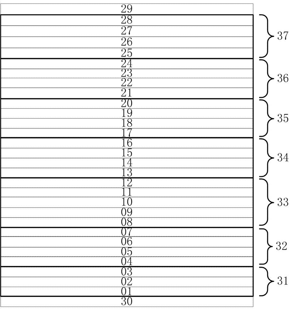
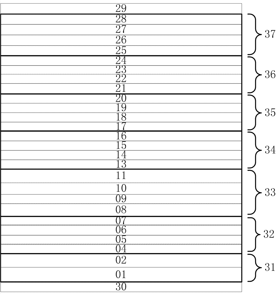
[0021] figure 1 Shown is a structural schematic diagram of a first embodiment of a GaInP / GaAs / Ge / Ge four-junction solar cell with a buffer layer.
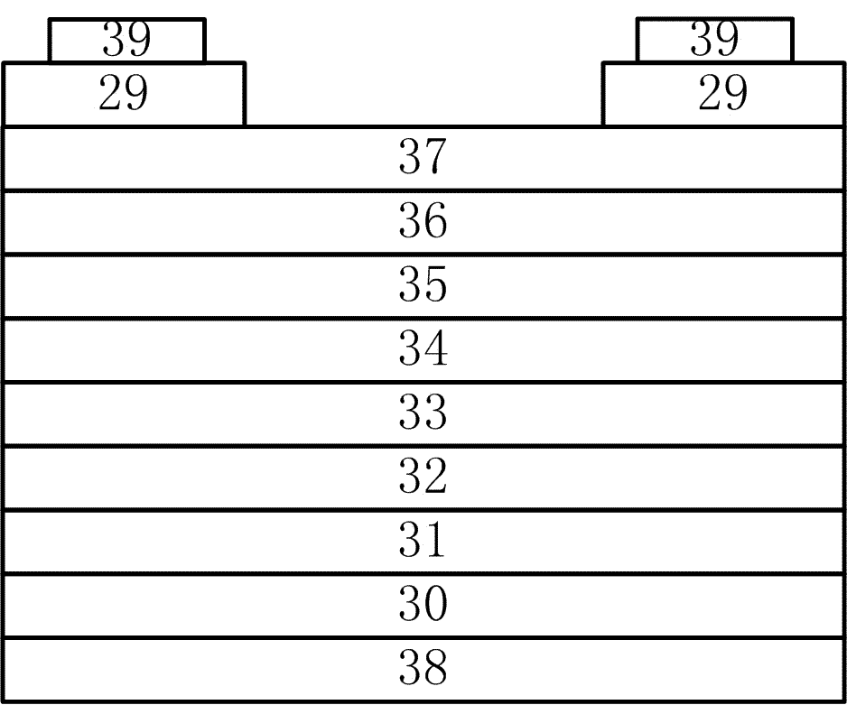
[0022] figure 2 Shown is a schematic diagram of the product structure of a first embodiment of a GaInP / GaAs / Ge / Ge four-junction solar cell.
[0023] image 3 Shown is a schematic structural diagram of a first embodiment of a GaInP / GaAs / Ge / Ge four-junction solar cell without a buffer layer.
[0024] This embodiment provides a GaInP / GaAs / Ge / Ge four-junction solar cell grown in a front-mount manner, and the bandgap combination is 1.90eV / 1.42eV / 0.67eV / 0.67eV. The structure of the GaInP / GaAs / Ge / Ge four-junction cell solar cell is as follows image 3 As shown, it includes a Ge substrate layer 30, and a first Ge subcell 31, a first tunnel junction 32, a second Ge subcell 33, a second tunnel junction 34, and a GaAs subcell arranged in sequence on the Ge substrate layer 30. A subcell 35 , a third tunnel junction 36 , a GaInP subcell 3...
no. 2 Embodiment approach
[0051] This embodiment provides a method for preparing a GaInP / GaAs / Ge / Ge four-junction solar cell using a front mounting method, such as Figure 4 shown, including:
[0052] Step 401, providing a substrate layer;
[0053] Step 402, growing a first Ge sub-cell on the surface of the Ge substrate layer;
[0054] Step 403, growing a first tunnel junction on the surface of the first Ge sub-cell;
[0055] Step 404, growing a second Ge sub-cell on the surface of the first tunnel junction;
[0056] Step 405, growing a second tunnel junction on the surface of the second Ge sub-cell;
[0057] Step 406, growing GaAs sub-cells on the surface of the second tunnel junction;
[0058] Step 407, growing a third tunnel junction on the surface of the GaAs sub-cell;
[0059] Step 408, growing GaInP sub-cells on the surface of the third tunnel junction;
[0060] Step 409, growing a contact layer on the surface of the GaInP sub-cell.
[0061] The above steps are grown by MOCVD (Metal Organi...
PUM
| Property | Measurement | Unit |
|---|---|---|
| Thickness | aaaaa | aaaaa |
Abstract
Description
Claims
Application Information
 - R&D Engineer
- R&D Manager
- IP Professional
- Industry Leading Data Capabilities
- Powerful AI technology
- Patent DNA Extraction
Browse by: Latest US Patents, China's latest patents, Technical Efficacy Thesaurus, Application Domain, Technology Topic, Popular Technical Reports.
© 2024 PatSnap. All rights reserved.Legal|Privacy policy|Modern Slavery Act Transparency Statement|Sitemap|About US| Contact US: help@patsnap.com