
Image sensor and its pixel readout method

An image sensor and pixel technology, which is applied in the direction of image communication, TV, color TV parts, etc., can solve the problems of easy image smear and low image quality, so as to improve dynamic range, reduce smear, and eliminate noise Effect

Active Publication Date: 2014-10-22
重庆艺鉴通文化艺术有限公司
View PDF3 Cites 0 Cited by
  • Summary
  • Abstract
  • Description
  • Claims
  • Application Information

AI Technical Summary

Problems solved by technology

[0011] The inventors of the present invention found that, in the prior art, the image sensor only includes one floating diffusion region, the captured image is prone to smear, and the image quality is not high enough

Method used


Image

  • Image sensor and its pixel readout method
  • Image sensor and its pixel readout method
  • Image sensor and its pixel readout method

Examples


Embodiment Construction

[0033] In the following description, many technical details are proposed in order to enable readers to better understand the application. However, those skilled in the art can understand that without these technical details and various changes and modifications based on the following implementation modes, the technical solution claimed in each claim of the present application can be realized.

[0034] In order to make the purpose, technical solution and advantages of the present invention clearer, the following will further describe the implementation of the present invention in detail in conjunction with the accompanying drawings.

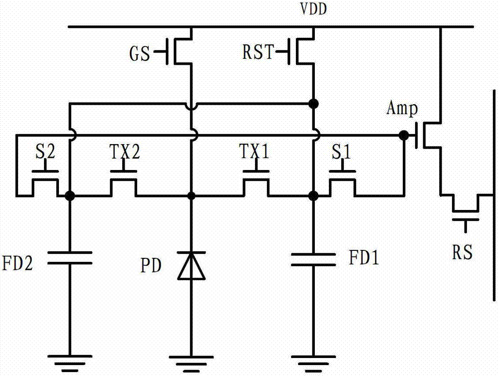
[0035] A first embodiment of the present invention relates to an image sensor. image 3 It is a schematic diagram of the circuit structure of the image sensor.

[0036] The image sensor includes: a controller and a plurality of pixel areas.

[0037] Specifically, as image 3 As shown, each pixel region includes a first floating diffusion region...


PUM


Abstract

The invention relates to the technical field of a semiconductor and discloses an image sensor and a pixel reading method thereof. In the invention, a transmission tube is added on a conventional CMOS (Complementary Metal Oxide Semiconductor) image sensor structure; two floating diffusion regions are formed by doping; and when the dynamic range of the image sensor is improved, an image tail is reduced. A long / short exposure mode is adopted, one image is exposed for a long time, the other image is exposed for a short time and then two images are synthesized so as to capture light details and dark details of the images, thereby improving the dynamic range of the image sensor. Images of an external flash device on the shining and non-shining phases are respectively acquired and then are synthesized, so that the light details and the dark details of the images can be simultaneously obtained and the image tail is reduced when dynamic range of the image sensor is improved. A correlated double sampling technology is adopted, i.e. signals which are sequentially read for twice are subtracted, so that the aim of eliminating the noise can be fulfilled.

Description

technical field [0001] The invention relates to the technical field of semiconductors, in particular to a metal oxide semiconductor image sensor with a double floating diffusion area structure with a global shutter. Background technique [0002] As we all know, an image sensor is a semiconductor device that converts an optical image into an electrical signal. Image sensors can be roughly classified into charge-coupled device (Charge-Coupled Device, “CCD” for short) and complementary metal oxide semiconductor (Complementary Metal Oxide Semiconductor, “CMOS” for short) image sensors. [0003] Existing CMOS image sensors include CMOS digital-to-analog circuits and pixel unit circuit arrays. [0004] According to its readout method, the existing CMOS image sensors can be roughly divided into passive pixel sensor (Passive Pixel Sensor, referred to as "PPS"), active pixel sensor (Active Pixel Sensor, referred to as "APS") and digital pixel sensor There are three types of sensors...

Claims


Application Information

Patent Timeline
Patent Type & Authority Patents(China)
IPC IPC(8): H04N5/369H04N5/355H04N5/357H04N5/374H01L27/146
Inventor 孙涛汪辉陈杰田犁方娜苗田乐
Owner 重庆艺鉴通文化艺术有限公司
Learn More