Output stage quick response circuit and response method thereof

A fast-response, output-stage technology, applied in the output-stage fast-response circuit, the fast-response of the above-mentioned output-stage fast-response circuit, in the field of fast-response circuits, can solve the problem that the rising edge time of the output signal of the output stage cannot be reduced, and the output transistor is turned off. Time without any help, etc., to achieve the effect of efficient rising edge and falling edge time process, reducing rising edge time, and accelerating state transition

Active Publication Date: 2014-09-03
赛卓电子科技(上海)股份有限公司
View PDF3 Cites 0 Cited by
  • Summary
  • Abstract
  • Description
  • Claims
  • Application Information

AI Technical Summary

Problems solved by technology

However, this circuit structure does not help the turn-off time of the output transistor, that is, it cannot reduce the rising edge time of the output signal of the output stage.

Method used


Image

  • Output stage quick response circuit and response method thereof
  • Output stage quick response circuit and response method thereof
  • Output stage quick response circuit and response method thereof

Examples


Embodiment 1

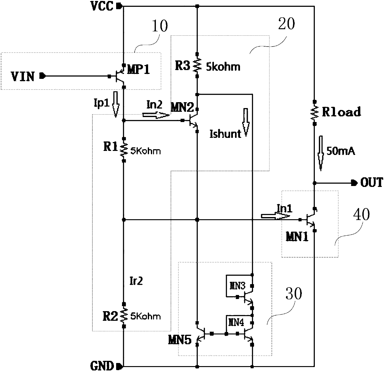
[0042] see image 3 , The present invention discloses a fast response circuit of an output stage, said circuit comprising: an input stage 10 , a driver stage 20 , an acceleration stage 30 , and an output stage 40 . This embodiment includes several transistors, and the transistors can be triodes based on bipolar technology, or MOS transistors based on CMOS technology; this embodiment uses the transistor as an example to introduce the fast response circuit of the present invention.

[0043] The input stage 10 is used for receiving an input signal VIN. In this embodiment, the input stage 10 includes a first triode MP1; the base of the triode MP1 is connected to the input signal terminal VIN, the collector is connected to the driving stage 20, and the emitter is connected to the power supply voltage VCC.

[0044] The output stage 40 includes a second transistor MN1 for outputting an output signal OUT. The base of the second transistor MN1 of the output stage is connected to the ...

Embodiment 2

[0060] see Figure 4 The difference between this embodiment and Embodiment 1 is that in this embodiment, the fast response circuit of the present invention uses a MOS transistor based on CMOS technology (replacing the triode in Embodiment 1) to realize the technical solution of the present invention.

[0061] The input stage is used for receiving the input signal VIN. The input stage includes a first MOS transistor MP1; the gate of the MOS transistor MP1 is connected to the input signal terminal VIN, the drain is connected to the driving stage, and the source is connected to the power supply voltage VCC.

[0062] The output stage includes a second MOS transistor MN1 for outputting an output signal OUT. The gate of the second MOS transistor MN1 of the output stage is connected to the second end of the first resistor R1, the drain of the second MOS transistor MN1 is connected to the signal output end, the second end of the fourth resistor Rload, and the second end of the fourth...


PUM


Abstract

The present invention discloses a fast response circuit of an output stage, said circuit comprising: an input stage, an output stage, a driver stage, and an acceleration stage; the acceleration stage is connected with the driver stage to reduce the rising edge of the output signal of the output stage time, falling edge time; the acceleration stage presets a preset amount of current, and when the second transistor MN1 of the output stage needs to be turned on, the preset current quickly flows into the second transistor MN1, thereby speeding up the turn-on time of the second transistor MN1 , reduce the falling edge time of the output signal; when the second transistor MN1 of the output stage needs to change from the on state to the off state, the acceleration stage quickly extracts excess carriers from the base of the second transistor MN1 of the output stage, accelerating state transition, reducing the rising edge time of the output signal. The output stage fast response circuit and its response method proposed by the invention can solve the problem that the rising edge time and falling edge time of the output stage signal in the analog integrated circuit are too long.

Description

technical field [0001] The invention belongs to the technical field of analog integrated circuit design, and relates to a quick response circuit, in particular to an output stage quick response circuit; meanwhile, the invention also relates to a quick response method of the output stage quick response circuit. Background technique [0002] The switching speed of the integrated circuit is a key parameter, which directly affects the operating frequency of the circuit. More importantly, to obtain a square wave close to the ideal, it is necessary to minimize the rising edge time and falling edge time. The rising and falling edge times reflected in the circuit are the times when a transistor transitions from the on state to the off state or from the off state to the on state. According to semiconductor physics and transistor principles, the transition of a transistor from an on state to an off state, and from an off state to an on state is a process of carrier flow, which takes a...

Claims


Application Information

Patent Timeline
Patent Type & Authority Patents(China)
IPC IPC(8): H03K19/01H03K19/094
Inventor 宋红刚徐威群陈婉付继祥
Owner 赛卓电子科技(上海)股份有限公司
Why Eureka
Try Eureka