
Method for predicting voltage value of full-open defect of interconnecting wire of deep sub-micron integrated circuit

An integrated circuit, deep sub-micron technology, used in electrical digital data processing, special data processing applications, instruments, etc., to solve problems such as missing contact holes or through holes, broken metal lines or through holes, and detection.

Inactive Publication Date: 2012-10-03
XI AN JIAOTONG UNIV
View PDF2 Cites 6 Cited by
  • Summary
  • Abstract
  • Description
  • Claims
  • Application Information

AI Technical Summary

Problems solved by technology

[0003] (1) Insufficient consideration of manufacturability design implied in layout design, such as insufficient insertion of multi-vias
[0004] (2) Defects introduced by etching steps during chip manufacturing
[0005] (3) Defects introduced by the etching step during chip manufacturing
[0006] (4) Contact holes or through holes are completely missing or incomplete during chip manufacturing
[0007] (5) Breakage of metal lines or vias due to electromigration effects
Since the voltage of the open-circuit defect point is no longer a fixed value, if we continue to use the above traditional static defect models: the model fixed at 0 (stuck-at 0), the model fixed at 1 (stuck-at 1), and multiple fixed In the case of N-detection stuck-at, it will be found that a large number of open-circuit defects can no longer be detected by the existing test vectors during the chip test stage, and the chip test coverage will no longer meet the requirements
Indeed, in the actual 90nm, 65nm, 45nm, 40nm, and 23nm projects, it has been found that more and more real open-circuit faults are missed, and the electrical performance of the chip is wrong but cannot be tested by existing tests. vector detected
Chip test engineers have to send these defective chips that cannot be tested to DFT engineers for Customer Retain analysis, which greatly wastes testing time
And even after entering the process of customer defective product return analysis, there is no reliable voltage prediction formula for open circuit defects, and there is no way to effectively diagnose, determine, and locate these defects, and there is still no way to achieve high test coverage

Method used


Image

  • Method for predicting voltage value of full-open defect of interconnecting wire of deep sub-micron integrated circuit
  • Method for predicting voltage value of full-open defect of interconnecting wire of deep sub-micron integrated circuit
  • Method for predicting voltage value of full-open defect of interconnecting wire of deep sub-micron integrated circuit

Examples


Embodiment Construction

[0054] The present invention is described in further detail below in conjunction with accompanying drawing:

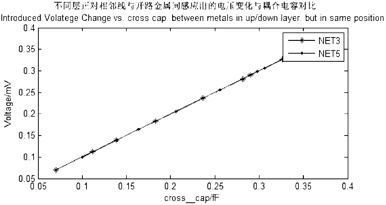
[0055] see Figure 1-11 , due to the deep submicron and ultra-deep submicron process conditions, there is a large coupling capacitance between other signal lines and open metal lines adjacent to the physical position of the open defect point in the integrated circuit layout (Layout). Under the influence of the coupling capacitance, when the logic states of other adjacent signal lines change, the voltage at the open-circuit defect also changes correspondingly. The voltage prediction method proposed in the present invention is to establish the relationship between the voltage of the open circuit point and the coupling capacitance, and use the coupling capacitance of the adjacent signal line to represent the voltage value and voltage logic of the circuit defect point.

[0056] The invention is based on the TSMC (TSMC) 40nm digital CMOS technology to simulate and analyze ...


PUM


Abstract

The invention discloses a method for predicting a voltage value of a full-open defect of an interconnecting wire of a deep sub-micron integrated circuit. By the method, the voltage at a full-open defect spot of an interconnecting wire can be accurately and efficiently determined in the designing stage of a chip. The method comprises the following steps of: establishing a first voltage prediction model, and establishing a second voltage prediction model based on the first voltage prediction model; extracting coupling capacitance values of peripheral signal wires of a metal wire which is suspected to have an open defect, and calculating a voltage logic by using the second voltage prediction model; and in the automatic test vector generating step of testability design, loading a test vector which is opposite to the calculated voltage logic, and finding the full-open defect on the metal wire if the situation that an open voltage logic is equal to the calculated value obtained by the second voltage prediction model is observed. The method has the advantages that two voltage models which are accurate and feasible in engineering are established, and a complete method for combining the two models is provided.

Description

Technical field: [0001] The invention belongs to the field of integrated circuits, and relates to a fault test method for testability design of integrated circuits, in particular to a method for predicting the full open circuit defect voltage value of deep submicron integrated circuit interconnection lines. Background technique: [0002] Open defect is one of the common failures in integrated circuits. Open-circuit defects may be introduced in chip design, manufacturing and application, resulting in errors in the electrical characteristics of the circuit. The main causes of open-circuit defects during chip physical design, tape-out steps, and chip application are: [0003] (1) Insufficient consideration of manufacturability design implicit in layout design, such as insufficient insertion of multi-vias. [0004] (2) Defects introduced by lithography steps during chip manufacturing. [0005] (3) Defects introduced by the etching step during chip manufacturing. [0006] (4)...

Claims


Application Information

Patent Timeline
IPC IPC(8): G06F17/50
Inventor 韦素芬邵志标耿莉
Owner XI AN JIAOTONG UNIV
Learn More