
Liquid crystal panel and manufacturing method thereof

A technology for a liquid crystal panel and a manufacturing method, which is applied in nonlinear optics, instruments, optics, etc., can solve the problems of increasing the size of the liquid crystal panel, the difficulty of designing a narrow frame, and the requirement of increasing the cutting accuracy, so as to improve the overflow and reduce the design difficulty. The effect of the requirement on panel cutting accuracy

Active Publication Date: 2012-10-03
TCL CHINA STAR OPTOELECTRONICS TECH CO LTD
View PDF6 Cites 37 Cited by
  • Summary
  • Abstract
  • Description
  • Claims
  • Application Information

AI Technical Summary

Problems solved by technology

In the existing technology, there is a certain precision error in the coating of the frame glue, and the physical state of the frame glue is non-solid. When the upper and lower substrates are pressed together, the frame glue will overflow to both sides, so that the width of the frame glue will increase.
Moreover, when cutting panels, there is also a certain accuracy error. In order to ensure the cutting effect, the frame glue must keep a certain distance from the cutting line to accommodate the accuracy error
However, if the frame glue is far away from the cutting line, the size of the LCD panel will be increased, making the narrow frame design more difficult, and also increasing the requirements for cutting accuracy

Method used


Image

  • Liquid crystal panel and manufacturing method thereof
  • Liquid crystal panel and manufacturing method thereof
  • Liquid crystal panel and manufacturing method thereof

Examples


Embodiment Construction

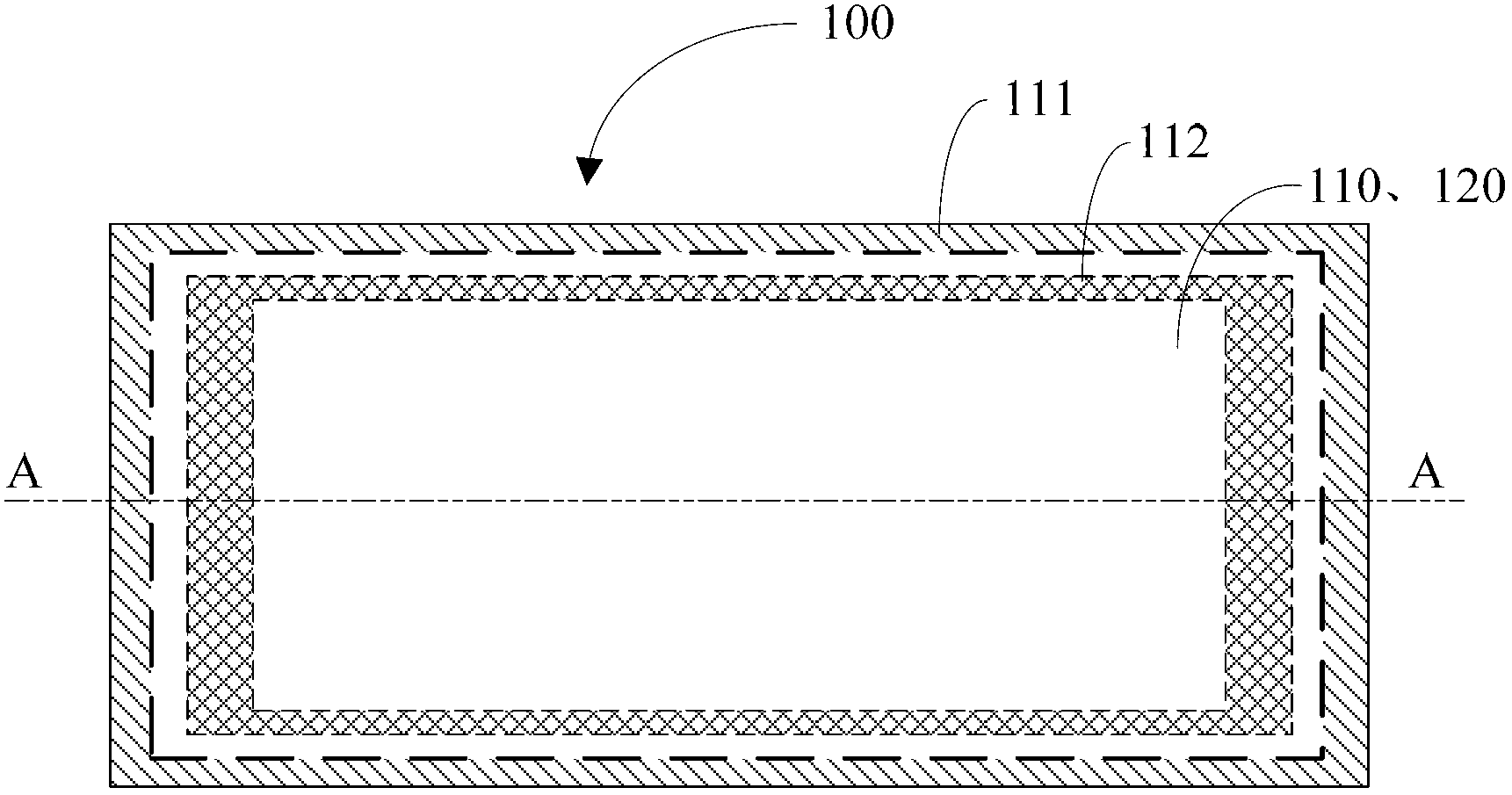
[0023] refer to figure 1 , figure 1 It is a top perspective schematic view of the liquid crystal panel according to the first embodiment of the present invention. figure 2 Yes figure 1 A schematic cross-sectional view of the liquid crystal panel in A-A.

[0024] Please also refer to figure 1 And and figure 2 As shown, in this embodiment, the liquid crystal panel 100 includes a first substrate 110 , a second substrate 120 , a retaining wall 111 , a sealant 112 and a liquid crystal 130 .

[0025] The first substrate 110 is opposite to the second substrate 120 .

[0026] In this embodiment, the first substrate 110 is a color filter substrate, and the second substrate 120 is a thin film transistor array substrate. Alternatively, the first substrate 110 is a thin film transistor array substrate, and the second substrate 120 is a color filter substrate. In other embodiments, the first substrate 110 may be an active element array substrate in other forms, and the second subs...


PUM


Abstract

The invention discloses a liquid crystal panel and a manufacturing method thereof. The liquid crystal panel comprises a first base plate, a second base plate, a frame glue and a retaining wall, wherein the first base plate and the second base plate are oppositely arranged; the frame glue is annularly arranged between the first base plate and the second base plate; the retaining wall is arranged between the first base plate and the second base plate and positioned outside an area surrounded by the frame glue, and the top surface and the bottom surface of the retaining wall respectively closely support against the first base plate and the second base plate. According to the mode, the flush of the frame glue can be avoided and the design difficulty of a narrow frame and the requirement of cutting accuracy can be lowered.

Description

technical field [0001] The invention relates to the field of display technology, in particular to a liquid crystal panel and a manufacturing method thereof. Background technique [0002] In recent years, various display technologies have continued to flourish, and products such as liquid crystal panels have been gradually commercialized and applied to display devices of various sizes. In the process of manufacturing the liquid crystal panel, it generally includes bonding the thin film transistor array substrate and the color filter substrate through a sealant. In the existing technology, there is a certain precision error in the coating of the frame glue, and the physical state of the frame glue is non-solid. When the upper and lower substrates are pressed together, the frame glue will overflow to both sides, so that the width of the frame glue will increase. . Moreover, when cutting panels, there is also a certain accuracy error. In order to ensure the cutting effect, the...

Claims


Application Information

Patent Timeline
IPC IPC(8): G02F1/1339G02F1/1333
CPCG02F1/1339
Inventor 陈政鸿王醉
Owner TCL CHINA STAR OPTOELECTRONICS TECH CO LTD
Learn More