Mounting device

A technology of mounting and mounting body, which is applied in the direction of lighting and heating equipment, electrical components, semiconductor/solid-state device manufacturing, etc., can solve the problems of space saving and other problems, and achieve space saving, cost reduction and low cost Effect

Inactive Publication Date: 2012-09-19
TOKYO ELECTRON LTD
View PDF7 Cites 4 Cited by
  • Summary
  • Abstract
  • Description
  • Claims
  • Application Information

AI Technical Summary

Problems solved by technology

[0009] However, using Figure 5 The mounting device such as the cooling and heating device 6 of the wafer chuck 1 shown requires a coolant tank 61, a first coolant circulation path 62, a second coolant circulation path 63, a first pump 62A, a second pump 63A, and a second pump 63A. The installation space of the Tring heat engine 66, etc. is a problem in terms of space saving as a cooling device used in the mounting device

Method used


Image

  • Mounting device
  • Mounting device
  • Mounting device

Examples


Embodiment Construction

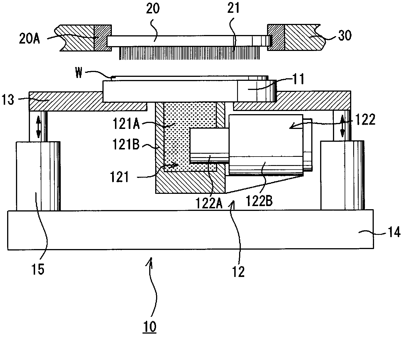
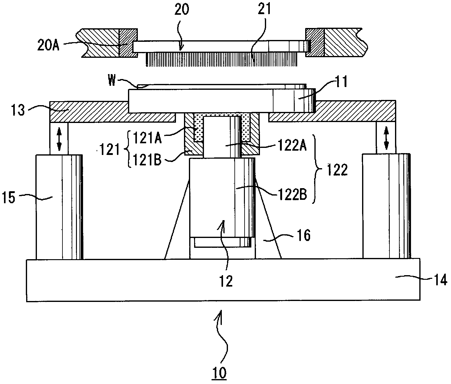
[0023] Below, based on Figure 1 ~ Figure 3 The illustrated embodiments illustrate the invention.

[0024] For example figure 1 As shown, the mounting device 10 of this embodiment includes: a mounting body (wafer chuck) 11 for mounting a semiconductor wafer W; a cooling mechanism 12 for cooling the semiconductor wafer through the wafer chuck 11 W; the support body 13, which supports the wafer chuck 11 at the outer peripheral edge of the wafer chuck 11; and the lifting mechanism 15, which supports the support body 13 at multiple positions in a manner that the support body 13 can be raised and lowered on the base 14 , the mounting device 10 is configured to be applied to, for example, an inspection device for inspecting electrical characteristics of a semiconductor wafer W. The above-mentioned lifting mechanism 15 may be constituted by a cylinder mechanism.

[0025] A probe card 20 is provided above the wafer chuck 11 . The probe card 20 is mounted on a top plate 30 forming...


PUM


Abstract

The present invention provides a mounting device capable of achieving cost reduction and space saving of a cooling mechanism for cooling a target object mounted on a mounting body. The mounting device (10) includes: a wafer chuck (11) for mounting thereon a wafer (W) for inspecting electrical characteristics of the wafer (W); and a cooling mechanism (12) for cooling the wafer (W) via the wafer chuck (11), wherein the cooling mechanism (12) includes a heat exchanger (121) provided at a bottom surface of the wafer chuck (11), and a cooling unit (122) having a heat absorbing unit (122A) for absorbing heat from a heat transfer medium (121A) of the heat exchanger (121), and wherein the cooling unit (122) is fixed to the heat exchanger (121) through the heat absorbing unit (122A).

Description

technical field [0001] The present invention relates to a mounting device having a cooling mechanism for cooling a processed object such as a semiconductor wafer to a predetermined temperature when processing a processed object such as a semiconductor wafer at a low temperature. In more detail, it relates to a A low-cost mounting device can be realized by simplifying the cooling mechanism. Background technique [0002] Conventional mounting devices are used in various processing devices in the field of semiconductor manufacturing. Here, an example of a mounting device used in an inspection device for inspecting electrical characteristics of a semiconductor wafer will be described. [0003] For the conventional inspection device E, for example, Figure 4 As shown, it includes: a loading chamber L, which is used to transport a semiconductor wafer W; a detector chamber (Japanese: プロババ chamber) P, which is used to inspect the electrical characteristics of the semiconductor wafe...

Claims


Application Information

Patent Timeline
Patent Type & Authority Applications(China)
IPC IPC(8): H01L21/67H01L21/66
CPCF25B9/14H01L21/67109H01L21/683H01L22/00
Inventor 山田浩史
Owner TOKYO ELECTRON LTD
Why Eureka
Try Eureka