Array base plate, preparation method of array base plate and liquid crystal display

An array substrate and a substrate technology, applied in the field of array substrates and their preparation, can solve the problems of poor Ion characteristics, slow charging speed, low brightness, etc., and achieve the effects of improving brightness, speeding up charging speed, and improving Ion characteristics

Inactive Publication Date: 2014-08-20
BEIJING BOE OPTOELECTRONCIS TECH CO LTD
View PDF4 Cites 0 Cited by
  • Summary
  • Abstract
  • Description
  • Claims
  • Application Information

AI Technical Summary

Problems solved by technology

[0005] Embodiments of the present invention provide an array substrate and its preparation method and a liquid crystal display, which are used to solve the problems of poor Ion characteristics, slow charging speed and low brightness of existing LCDs

Method used


Image

  • Array base plate, preparation method of array base plate and liquid crystal display
  • Array base plate, preparation method of array base plate and liquid crystal display
  • Array base plate, preparation method of array base plate and liquid crystal display

Examples


Embodiment 1

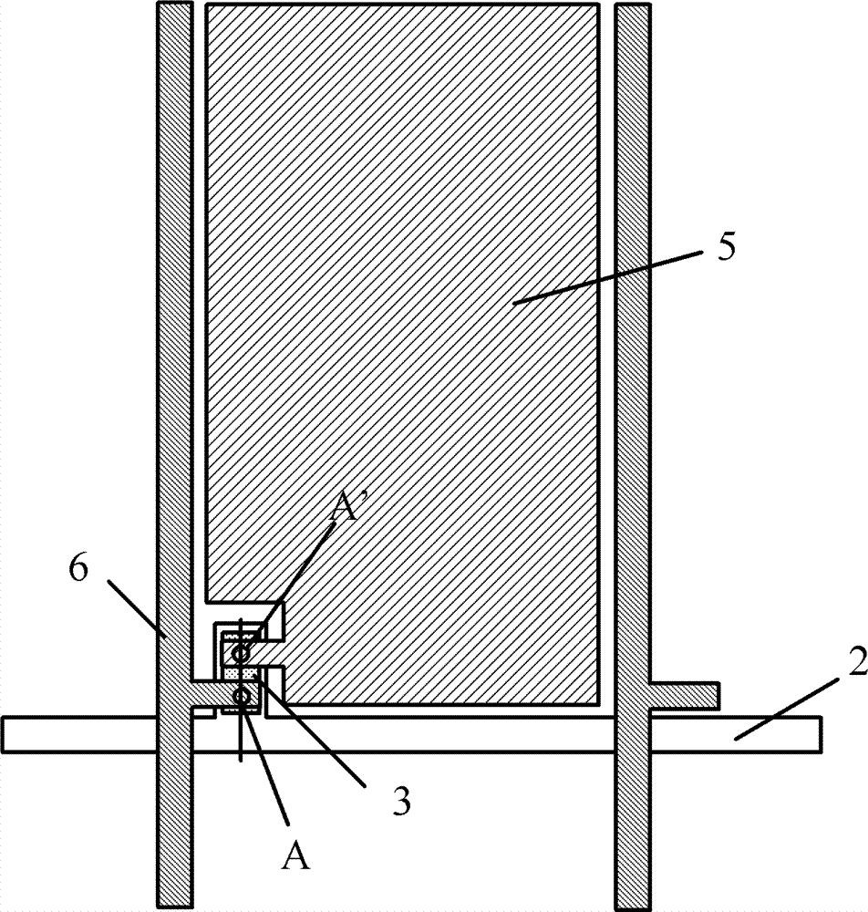
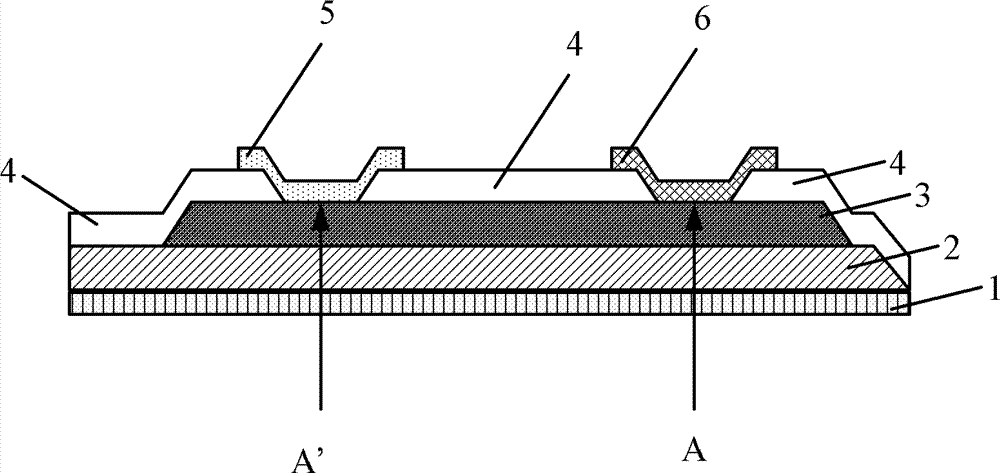
[0030] Embodiment 1 of the present invention provides an array substrate, and the structure diagram of the array substrate is as follows: figure 1 as shown, figure 1 A schematic structural diagram of a pixel region in the array substrate is specifically shown in . The array substrate for figure 1 A schematic cross-sectional view of a pixel region shown in figure 2 shown.

[0031] The array substrate includes a substrate 1, on which a control electrode layer 2, a giant magnetoresistance layer 3, an insulating layer 4, a pixel electrode layer 5 and a signal electrode layer 6 are sequentially deposited in a direction from close to the substrate 1 to away from the substrate 1, Wherein, the control electrode layer 2 , the giant magnetoresistance layer 3 and the insulating layer 4 together form a giant magnetoresistance active matrix.

[0032] For each pixel area, the insulating layer 4 is provided with two via holes, the signal electrode layer 6 is connected to the giant magne...

Embodiment 2

[0049] Embodiment 2 of the present invention provides a method for preparing an array substrate, such as Figure 4 Shown is the step flowchart of this method, and this method comprises:

[0050] Step 101, forming a control electrode layer.

[0051] This step includes: depositing a transparent conductive film on the substrate, forming a control electrode layer pattern on the transparent conductive film, and crystallizing the control electrode layer pattern, that is, crystallizing the control electrode layer pattern.

[0052] Preferably, the material of the transparent conductive film can be indium tin oxide ITO, and the transparent conductive film can be deposited by magnetron sputtering on the cleaned substrate, and formed on the transparent conductive film through the exposure etching process. Control the pattern of the electrode layer, and crystallize the pattern of the control electrode layer through an annealing process.

[0053] Step 102, forming a giant magnetoresistan...

Embodiment 3

[0069] Embodiment 3 of the present invention also provides a liquid crystal display including the array substrate provided in Embodiment 1 of the present invention.


PUM


Abstract

An array substrate, a method for preparing same, and a display device. The array substrate comprises a substrate (1) and a control electrode layer (2), a giant magnetoresistance layer (3), an insulating layer (4), a pixel electrode layer (5) and a signal electrode layer (6) sequentially provided on the substrate (1) in the direction from near the substrate (1) away from the substrate (1). The control electrode layer (2) comprises a control electrode line (21) and a control electrode (22), and the control electrode line (21) and the control electrode (22) are electrically connected or integrated. The signal electrode layer (6) comprises a signal electrode line (61) and a signal electrode (62), and the signal electrode line (61) and the signal electrode (62) are electrically connected or integrated. The pixel electrode layer (5) comprises a plurality of pixel electrodes (51). The control electrode line (21) and the signal electrode line (61) intersect each other to define pixel units arranged into a matrix. Each pixel unit comprises a pixel electrode (51) and a giant magnetoresistance layer (3). In each pixel unit, the signal electrode (62) is connected to the giant magnetoresistance layer (3), and the pixel electrode (51) is connected to the giant magnetoresistance layer (3). Therefore, the on-state current characteristic of the display device is effectively increased, so as to increase the charging speed and increase the brightness.

Description

technical field [0001] The invention relates to the technical field of liquid crystal displays, in particular to an array substrate, a preparation method thereof, and a liquid crystal display. Background technique [0002] The traditional thin-film transistor liquid crystal display (TFT-LCD, Thin-Film Technology Liquid Crystal Display) occupies a dominant position in the flat panel display market due to its low power consumption and low radiation characteristics. The core component of TFT-LCD is thin-film transistor TFT electrode. Due to the complex preparation process of polysilicon TFT electrode and the disadvantages that it cannot be prepared in a large area, the vast majority of TFT-LCDs currently use hydrogenated amorphous silicon thin-film transistors. [0003] However, hydrogenated amorphous silicon TFT has poor characteristics, especially the low on-state current (Ion), which leads to poor Ion characteristics of liquid crystal displays, and the charging speed of liqu...

Claims


Application Information

Patent Timeline
Patent Type & Authority Patents(China)
IPC IPC(8): G02F1/1362H01L27/22H01L21/77
CPCG02F1/1362
Inventor 张金中
Owner BEIJING BOE OPTOELECTRONCIS TECH CO LTD
Why Eureka
Try Eureka