Array substrate, dual field of view display device and manufacturing method thereof
A dual-view field display and array substrate technology, which is applied in semiconductor/solid-state device manufacturing, optics, instruments, etc., can solve the problems of increased production costs, lower substrate yield and reliability, and improve yield and reliability , reduce production costs, and expand the effect of visual range
- Summary
- Abstract
- Description
- Claims
- Application Information
AI Technical Summary
Problems solved by technology
Method used
Image
Examples
Embodiment 1
[0051] An embodiment of the present invention provides an array substrate, such as Figure 4a As shown, it includes a plurality of pixel units 43 divided by crossing gate lines 41 and data lines 42 , and each pixel unit 43 includes a pixel electrode 431 and a TFT circuit 432 .
[0052] The pixel electrode 431 of each pixel unit 43 includes at least two first pixel electrodes 4311 and at least two second pixel electrodes 4312 spaced apart from each other.
[0053] The TFT circuit 432 of each pixel unit 43 includes a first sub-TFT circuit 4321 connected to the first pixel electrode 4311 and a second sub-TFT circuit 4322 connected to the second pixel electrode 4312 . That is, all the first pixel electrodes 4311 are connected to the first sub-TFT circuit 4321 , and all the second pixel electrodes 4312 are connected to the second sub-TFT circuit 4322 . Wherein, each first pixel electrode 4311 can be connected to the first sub-TFT circuit 4321 through any structure that can realize...
Embodiment 2
[0063] The embodiment of the present invention and the following embodiment three provide a dual-view field display device, using the array substrate as described in the above-mentioned embodiment 1, including a dual-view field liquid crystal display device and a dual-view field OLED display device . Wherein, the first field of view pixel electrode described in the following embodiments corresponds to the first pixel electrode in the array substrate described in Embodiment 1; the second field of view pixel electrode corresponds to the first pixel electrode in the array substrate described in Embodiment 1. the second pixel electrode.
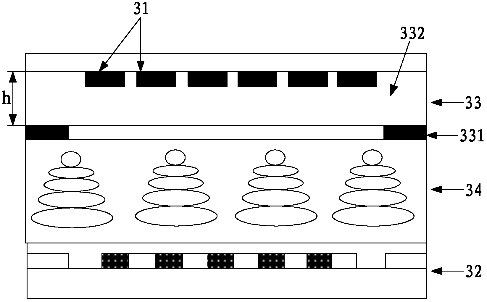
[0064] The dual-view field liquid crystal display device provided by the embodiment of the present invention uses the array substrate as described in the above-mentioned embodiment 1, such as image 3 shown, including:
[0065] Double-view baffle 31, TFT array substrate 32 and color filter substrate 33 formed in a box, wherein liquid crystal 34...
Embodiment 3
[0085] The dual-view OLED display device provided by the embodiment of the present invention uses the pixel unit structure of the array substrate described in the first embodiment, as Figure 9a As shown, it includes: a double-view baffle 91, a TFT array substrate 92 and a packaging layer 93, wherein the TFT array substrate 92 is as Figure 9b As shown, it includes a plurality of pixel units 96 divided by gate lines 94 and data lines 95 that intersect horizontally and vertically, and each pixel unit 96 includes an EL layer 97 and a control circuit 98 .
[0086] Such as Figure 9a As shown, the EL layer 97 includes a metal cathode 971, a pixel electrode 972, and an organic luminescent material 973 between the metal cathode 971 and the pixel electrode 972, and the pixel electrode 972 of each pixel unit 96 includes at least two first viewing electrodes spaced apart from each other. A field pixel electrode 9721 and at least two second viewing field pixel electrodes 9722 .
[008...
PUM
| Property | Measurement | Unit |
|---|---|---|
| Width | aaaaa | aaaaa |
| Thickness | aaaaa | aaaaa |
Abstract
Description
Claims
Application Information
 - R&D
- Intellectual Property
- Life Sciences
- Materials
- Tech Scout
- Unparalleled Data Quality
- Higher Quality Content
- 60% Fewer Hallucinations
Browse by: Latest US Patents, China's latest patents, Technical Efficacy Thesaurus, Application Domain, Technology Topic, Popular Technical Reports.
© 2025 PatSnap. All rights reserved.Legal|Privacy policy|Modern Slavery Act Transparency Statement|Sitemap|About US| Contact US: help@patsnap.com


