Negative voltage conversion circuit
A negative voltage, conversion circuit technology, applied in the direction of logic circuit connection/interface layout, logic circuit coupling/interface using field effect transistors, etc., can solve the problems of single supply, increase circuit area, disadvantageous circuit integration, etc., to avoid Breakdown, the effect of improving reliability
- Summary
- Abstract
- Description
- Claims
- Application Information
AI Technical Summary
Problems solved by technology
Method used
Image
Examples
Embodiment Construction
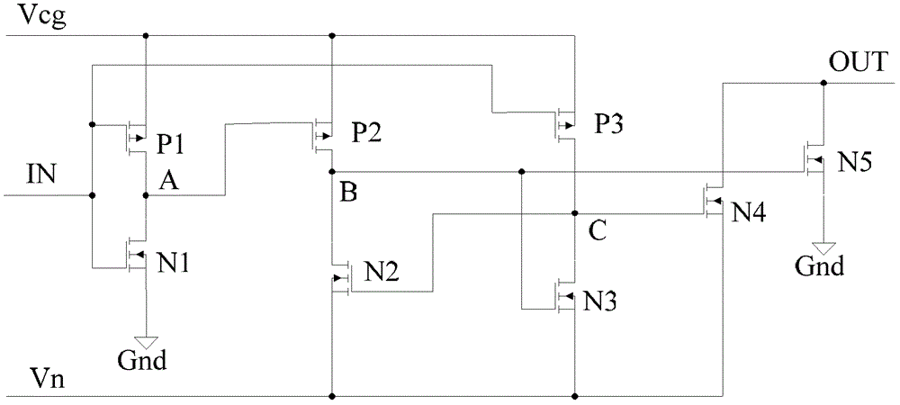
[0045] It can be seen from the background art that in the negative voltage conversion circuit of the prior art, the MOS transistor is likely to be broken down, thereby affecting the reliability of the circuit. Moreover, the negative conversion circuit in the prior art also requires a voltage converter to perform voltage conversion to achieve the positive voltage Vcg in the negative voltage circuit, which also makes the circuit area larger, which is not conducive to circuit integration.
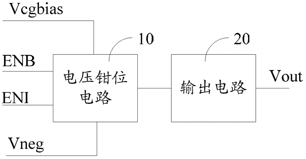
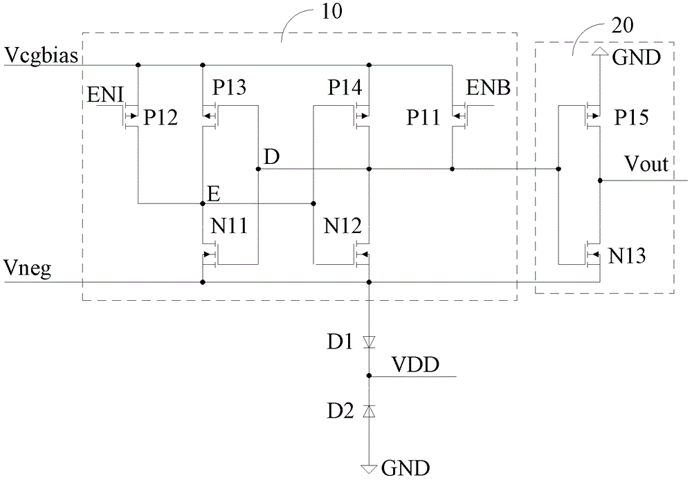
[0046] In the negative voltage conversion circuit of the present invention, when the negative voltage drops to a preset voltage value, the forward voltage drops from the first voltage value to the second voltage value, thereby reducing the required voltage between the poles of the MOS tubes in the circuit. The withstand voltage value prevents the MOS tube from being broken down, thereby improving the reliability of the circuit. On the other hand, the first voltage value of the forward voltage ...
PUM
 Abstract
Description
Claims
Application Information
 - R&D Engineer
- R&D Manager
- IP Professional
- Industry Leading Data Capabilities
- Powerful AI technology
- Patent DNA Extraction
Browse by: Latest US Patents, China's latest patents, Technical Efficacy Thesaurus, Application Domain, Technology Topic, Popular Technical Reports.
© 2024 PatSnap. All rights reserved.Legal|Privacy policy|Modern Slavery Act Transparency Statement|Sitemap|About US| Contact US: help@patsnap.com


