
Display panel and source driving structure thereof

一种显示面板、源极驱动的技术,应用在静态指示器、仪器等方向,能够解决成本低、驱动开关横向空间限制、多纵向空间等问题,达到负载差异减少、解决显示画面不协调的效果

Inactive Publication Date: 2012-04-18
AU OPTRONICS CORP
View PDF5 Cites 11 Cited by
  • Summary
  • Abstract
  • Description
  • Claims
  • Application Information

AI Technical Summary

Problems solved by technology

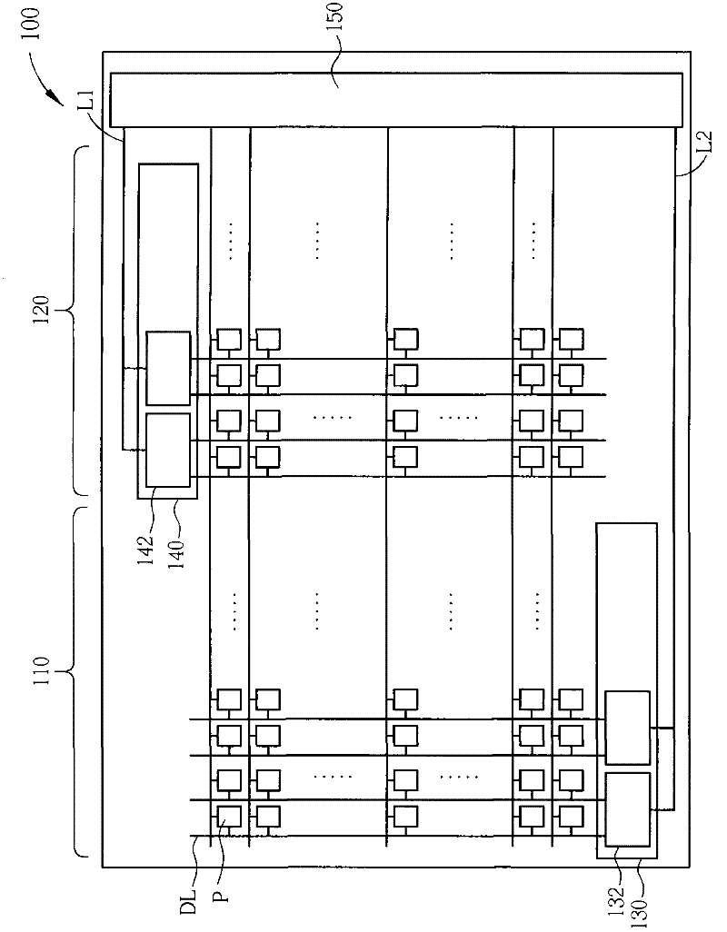
[0003] However, according to the above configuration, the driving switches 132, 142 of the multiplexers 130, 140 are adjacent to each other, causing the horizontal space of the driving switches to be limited, so the driving switches of the multiplexer will occupy more vertical space. , and then increase the required width of the upper and lower side edges of the display panel 100, and relatively, other places where the multiplexer is not provided on the upper and lower side edges cause a waste of space
In addition, the length of the signal line L2 electrically connected to the multiplexer 130 is longer than the length of the signal line L1 electrically connected to the multiplexer 140, so the load of the pixel P on the right half and the pixel on the left half There is a difference in the load of P, which may easily cause uncoordinated display images on the left and right sides of the display panel 100
[0004] Furthermore, transistors made of indium gallium zinc oxide (InGaZn Oxide, IGZO) have the advantages of high electron movement speed, so the current driving ability is high, so they can be used as the material for the display device driving circuit, made by IGZO The advantage of the transistor is that the number of photomasks is less, the cost is lower than that of the LTPS process, and the surface flatness of the TFT substrate is better. However, the electron movement speed of IGZO is lower than that of LTPS, so IGZO is used in multiplexer components. In terms of design, it occupies a relatively large area. When it is used in a high-resolution display device, it needs to consider its spatial configuration.

Method used


Image

  • Display panel and source driving structure thereof
  • Display panel and source driving structure thereof
  • Display panel and source driving structure thereof

Examples


Embodiment Construction

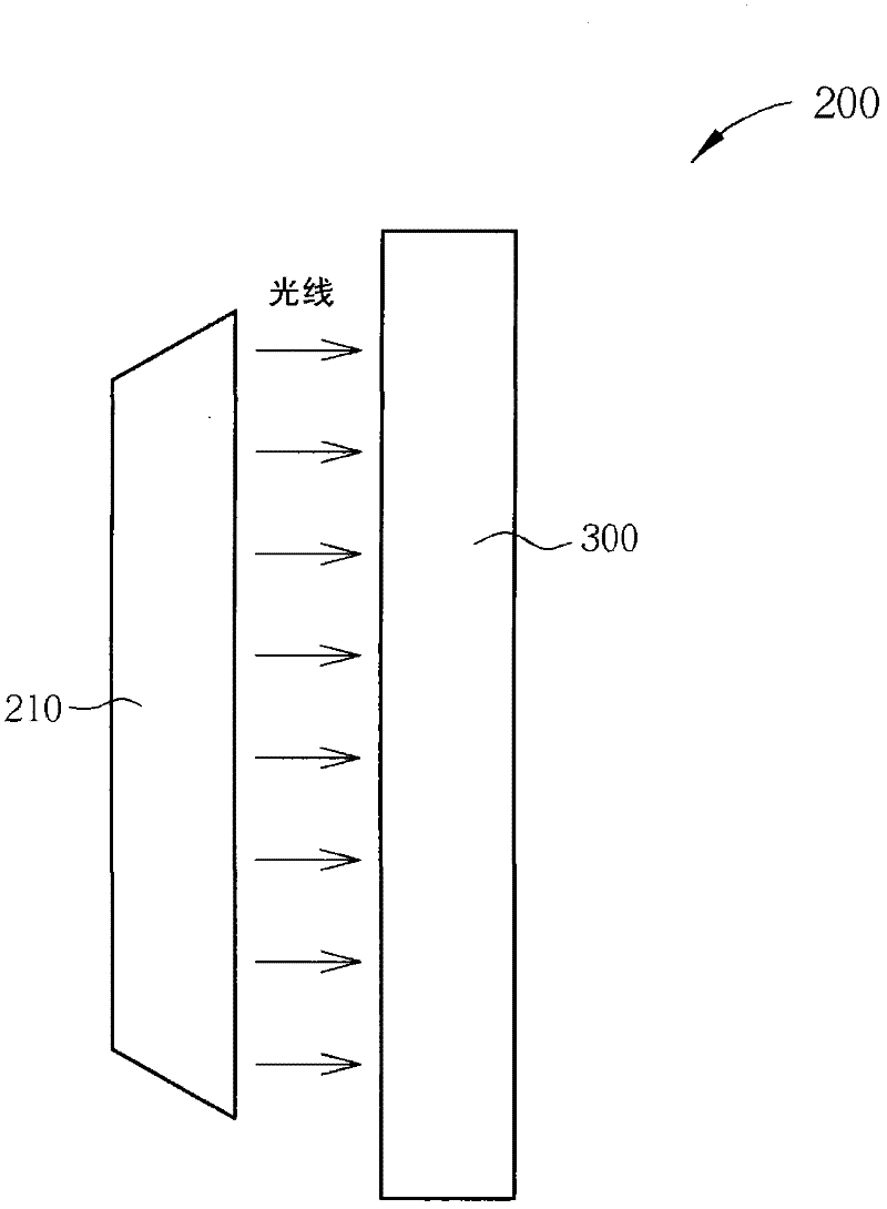
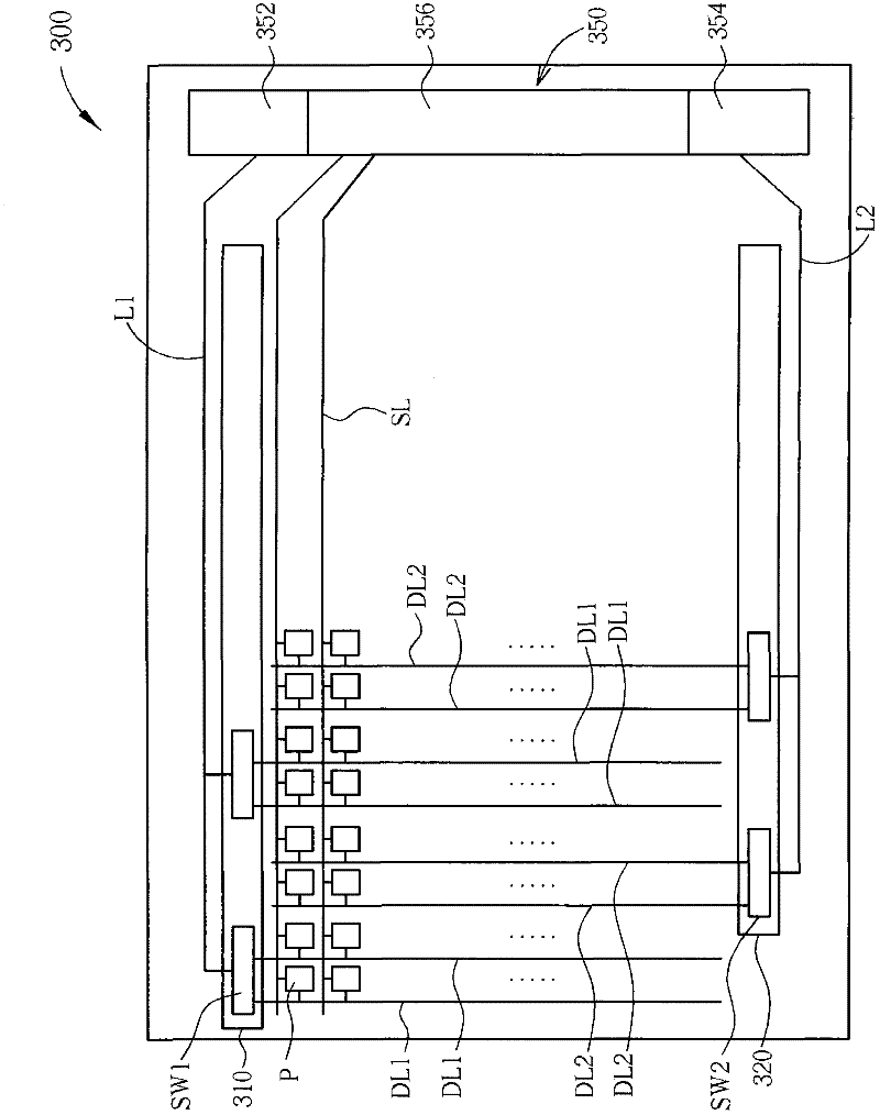
[0044] Please also refer to Figure 2 to Figure 4 . figure 2 It is a schematic diagram of the display of the present invention, image 3 for figure 2 A schematic diagram of a first embodiment of a display panel of a display, Figure 4 is a schematic diagram of the first embodiment of the driving switch of the multiplexer of the present invention. The display 200 includes a display panel 300 for displaying images, and a backlight module 210 for generating backlight. The display panel 300 includes a first multiplexer 310, a second multiplexer 320, a driving circuit 350, a plurality of first data lines DL1, a plurality of second data lines DL2, a plurality of scanning lines SL, and a plurality of pixel P. The first multiplexer 310 is disposed on the upper side of the display panel 300, and the first multiplexer 310 includes a plurality of first driving switches SW1. Each first driving switch 312 includes a first input terminal IN1, a plurality of first control terminals C...


PUM


Abstract

The invention provides a display panel and a source driving structure thereof. The display panel includes a plurality of first driving switches which are arranged on a first side of the display panel, a plurality of second driving switches which are arranged on a second side of the display panel, a plurality of first data lines, a plurality of second data lines, a plurality of scanning lines, and a plurality of pixels. Each first driving switch includes a first input terminal and a plurality of first output terminals. Each second driving switch includes a second input terminal and a plurality of second output terminals. The first data lines are electrically connected with the first output terminals. The second data lines are electrically connected with the second output terminals. The pixels are electrically connected with the first data lines, the second data lines, and the scanning lines, and are used to display pictures. The first data lines and the second data lines are staggered. The display panel and the source driving structure thereof can solve the picture discordance problem and the large area occupation problem caused by the application of the IGZO.

Description

technical field [0001] The present invention relates to a display panel, in particular to a source driving structure of the display panel. Background technique [0002] Please refer to figure 1 , figure 1 is a schematic diagram of a known display panel 100 . The display panel 100 is divided into a plurality of display blocks 110 and 120 , and the display blocks 110 and 120 are controlled by multiplexers 130 and 140 respectively. The multiplexers 130 and 140 are electrically connected to the driving circuit 150 for receiving the source driving signal generated by the driving circuit 150 . The driving switches 132 and 142 of the multiplexers 130 and 140 then transmit the source driving signals to the pixels P turned on by the scan lines SL through the data lines DL, so that the pixels P display images according to the source driving signals. Such as figure 1 As shown, the multiplexer 140 is disposed on the upper side of the display panel 100 for transmitting the source dr...

Claims


Application Information

Patent Timeline
Patent Type & Authority Applications(China)
IPC IPC(8): G09G3/20
CPCG09G3/20G09G2310/0218G09G2310/0275G09G2310/0281G09G2310/0297
Inventor 洪义轩丁友信陈振铭陈思洁范大伟傅春霖
Owner AU OPTRONICS CORP
Learn More