
Ion source cleaning in semiconductor processing systems

An ion implantation, indirect technology used in semiconductor/solid state device manufacturing, ion beam tubes, ion implantation plating, etc. to solve problems such as limiting commercial viability

Active Publication Date: 2014-08-27
ENTEGRIS INC
View PDF17 Cites 0 Cited by
  • Summary
  • Abstract
  • Description
  • Claims
  • Application Information

AI Technical Summary

Problems solved by technology

[0021] The use of fluorine-based or fluorine-containing interhalogen compounds for cleaning semiconductor processing equipment has associated deficiencies that limit its commercial viability

Method used


Image

  • Ion source cleaning in semiconductor processing systems
  • Ion source cleaning in semiconductor processing systems
  • Ion source cleaning in semiconductor processing systems

Examples


example 1

[0171] This example shows improvements in ion source lifetime and implanter utilization that can be achieved by using a chemical cleaner to remove deposits. Preferably, the deposits are removed at regular intervals in order to prevent the accumulation of contaminant flakes and conductive films in the implanter.

[0172] In-situ cleaning is performed at regular intervals from the XeF located in the gas box of the ion implanter. 2 The supply container introduces XeF 2 to carry out, where XeF 2 Purge vapors were introduced into the ion source twice daily for 10-15 minutes each. Experiments were performed using a high current implanter to evaluate the flow kinetics of the cleaning reagent. Identified XeF 2 Cleaning properties and demonstrated that the cleaning agent has no adverse effect on the beam tubing components of the implanter. Therefore, using XeF 2 The reagent cleaning procedure is qualified for use in a moderate current implanter device.

[0173] figure 1 is a gr...

example 2

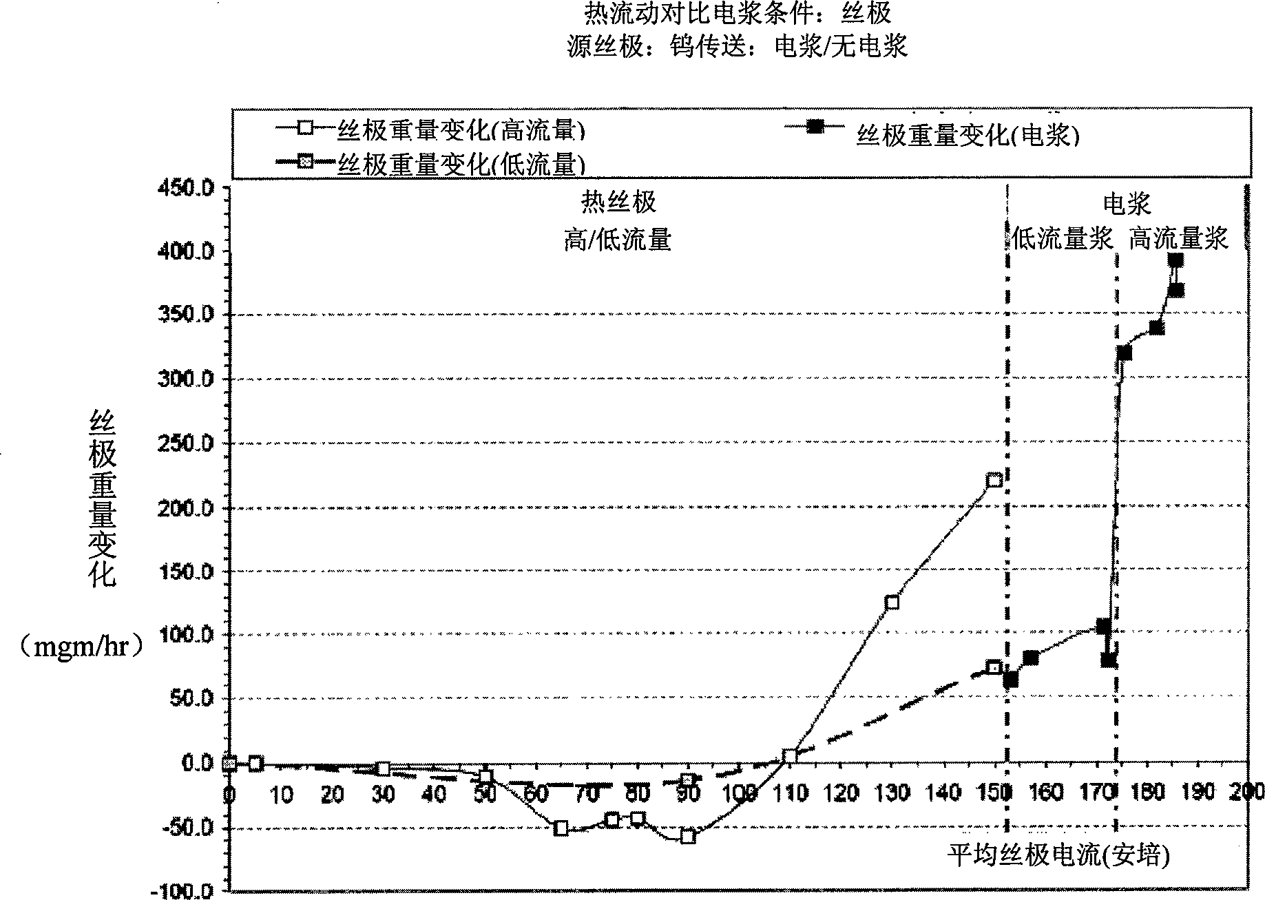
[0188] This example demonstrates the control of filament growth in the ion source of an illustrative ion implanter system.

[0189] Figure 5A shows the XeF in terms of increased filament current and weight 2 A diagram of the effects of current and arc power variations. The figure shows a plot of filament weight (in grams) as a function of elapsed time (in hours) of operation of the implanter system. The upper line in this graph represents XeF at 2.2 standard cubic centimeters per minute (sccm) 2 Flow rate and arc power operation of 100 volts / 0.05 amps, for which a filament weight gain of 319 mg / hour was determined after 3 hours of operation. The lower line in this graph reflects the XeF at 0.5 sccm 2 Flow rate and arc power of 40 volts / 0.05 amps, which produced a filament weight gain of 63 mg / hour over a 3 hour continuous execution time.

[0190] Figure 5B shows the XeF in terms of filament current 2 A diagram of the effect of flow and arc power changes. The figure s...


PUM


Abstract

The present invention relates to temperature and / or reactive cleaning by utilizing the temperature and / or reactive cleaning of a cathode capable of growing / etching an indirectly heated cathode in an ion implantation system by monitoring the cathode bias power and taking corrective action depending on the comparison value Reagents are used to etch or regrow the cathode to clean an ion implantation system or components thereof.

Description

technical field [0001] The present invention relates to the monitoring, control and cleaning of material deposition on components of semiconductor processing systems, particularly ion implantation systems. Background technique [0002] Ion implantation is used in the fabrication of integrated circuits to precisely introduce controlled amounts of dopant impurities into semiconductor wafers and is an important process in microelectronics / semiconductor production. In such implant systems, an ion source ionizes a desired dopant element gas into ions and the plasma is extracted from the source in the form of an ion beam of desired energy. Extraction is achieved by applying a high voltage across suitably shaped extraction electrodes that incorporate a plurality of apertures into the channels of the extraction beam. The ion beam is then directed at the surface of a workpiece, such as a semiconductor wafer, to implant dopant elements into the workpiece. The ions in the beam penetr...

Claims


Application Information

Patent Timeline
Patent Type & Authority Patents(China)
IPC IPC(8): H01L21/265
CPCH01J2237/22H01J27/08C23C14/564H01J2237/0209H01J37/08H01J37/18H01J2237/022H01J37/3171H01J37/16H01J2237/082C23C14/48C23C14/54H01J37/32862
Inventor 约瑟·D·史威尼莎拉德·N·叶达夫欧利格·拜罗伯·金姆大卫·艾德瑞吉丰琳史蒂芬·E·毕夏普W·卡尔·欧兰德唐瀛
Owner ENTEGRIS INC
Learn More