Current balancing of parallel connected semiconductor components

A technology for power semiconductors and components, which is applied in the field of current balance of semiconductor components connected in parallel, can solve problems such as difficult physical structure and complicated maintenance, and achieve the effect of small size and light weight

Active Publication Date: 2015-03-04
ABB (SCHWEIZ) AG
View PDF4 Cites 0 Cited by
  • Summary
  • Abstract
  • Description
  • Claims
  • Application Information

AI Technical Summary

Problems solved by technology

Such an arrangement and design results in additional material, development and manufacturing costs
Furthermore, such designs result in physical structures that make repair of the device complex and difficult

Method used


Image

  • Current balancing of parallel connected semiconductor components
  • Current balancing of parallel connected semiconductor components
  • Current balancing of parallel connected semiconductor components

Examples


Embodiment Construction

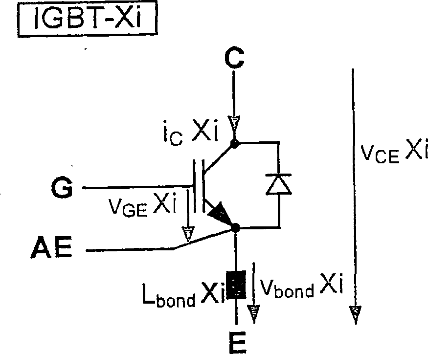
[0026] figure 1 Graphical symbols are shown with associated symbols and defined IGBT components used throughout. The IGBT component is denoted Xi, and it comprises a collector C terminal, a gate G terminal and an emitter E terminal. Furthermore, the part has an auxiliary emitter AE connected to the same potential as the emitter E and intended to be connected to a driver circuit or gate unit so that a suitable Voltage is used to control the part.

[0027] figure 1 Another definition in is the collector current i C,Xi , gate-to-emitter voltage v GE,Xi and collector to emitter voltage v CE,Xi . L bond,Xi is the stray inductance of the switching path of the part, and V bond,Xi is the voltage across this stray inductance.

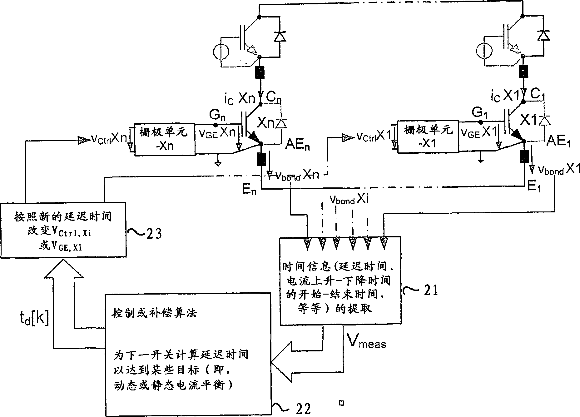
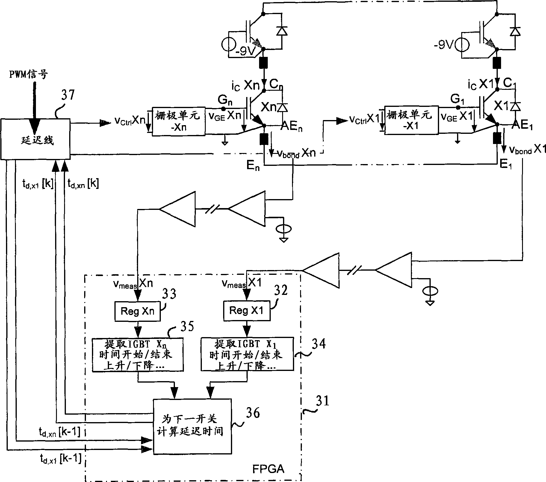
[0028] In an embodiment of the method, the semiconductor components connected in parallel are provided with switching signals for changing the state of the components. The switching signal is triggered by the control system of the device implementing t...


PUM


Abstract

1. A method and an arrangement of balancing switching transient behaviour of parallel connected power semiconductor components. The method comprises steps of providing a switch signal (s) to the parallel connected power semiconductor components (Xi) for changing the state of the components, forming control signals for each of the parallel connected components from the switch signal, determining during the change of state of the power semiconductor component the voltage induced to an inductance in the main current path of the component in each of the parallel connected components, comparing each of the induced voltages with a predetermined threshold voltage, measuring time differences between the time instants at which the induced voltages crosses the threshold voltage, and modifying one or multiple of the control signals on the basis of the measured time differences in the respective following state change for balancing the switching transient behaviour.

Description

technical field [0001] The present invention relates to the balancing of the currents of semiconductor components connected in parallel, in particular to balancing the currents in dynamic situations. Background technique [0002] The ever-increasing requirements for large power ratings and physically limited maximum current densities of semiconductor devices are why parallel connections of semiconductors are attractive for high-power applications. Parallel connection of power semiconductor components such as IGBTs (Insulated Gate Bipolar Transistors) is a widely spread solution for high power converters. In parallel operation of IGBTs, each parallel connected component receives a switching signal. The switching signal may e.g. emanate from a modulator used to determine the proper timing for the switching to occur. The switching signal is divided into a control signal for controlling each parallel-connected component. Therefore, the intent is to operate the switches simult...

Claims


Application Information

Patent Timeline
Patent Type & Authority Patents(China)
IPC IPC(8): H02M1/06
CPCH03K17/082H03K17/042H03K17/12
Inventor 罗德里戈·阿隆索·阿尔瓦雷斯瓦伦祖埃拉卡斯滕·芬克斯特芬·贝尔内特安东尼奥·科恰
Owner ABB (SCHWEIZ) AG
Why Eureka
Try Eureka