Pollution prevention device

An anti-pollution and ventilation tube technology, which is applied in the direction of electrical components, semiconductor/solid-state device manufacturing, circuits, etc., can solve problems that affect the quality of the wafer, contamination of the back and edge of the wafer, and the quality of the wafer cannot be further improved, so as to prevent the formation of defects. Effect

Active Publication Date: 2012-02-22
BEIJING NAURA MICROELECTRONICS EQUIP CO LTD
View PDF8 Cites 4 Cited by
  • Summary
  • Abstract
  • Description
  • Claims
  • Application Information

AI Technical Summary

Problems solved by technology

During the wafer cleaning process, chemical reagents and cleaning products easily enter the back of the wafer along the edge of the wafer, causing contamination on the back and edge of the wafer. If this pollution cannot be removed in time, it will cause defects on the back and edge of the wafer, especially in the subsequent high-temperature treatment. During the process of processing, the pollutants on the back and edge will diffuse to the front, seriously affecting the quality of the wafer. However, in the existing technology, there is no device that can effectively prevent the contamination of the back and edge of the wafer, so that the quality of the wafer cannot be further improved.

Method used


Image

  • Pollution prevention device
  • Pollution prevention device
  • Pollution prevention device

Examples


Embodiment Construction

[0022] The specific implementation manners of the present invention will be further described in detail below in conjunction with the accompanying drawings and embodiments. The following examples are used to illustrate the present invention, but are not intended to limit the scope of the present invention.

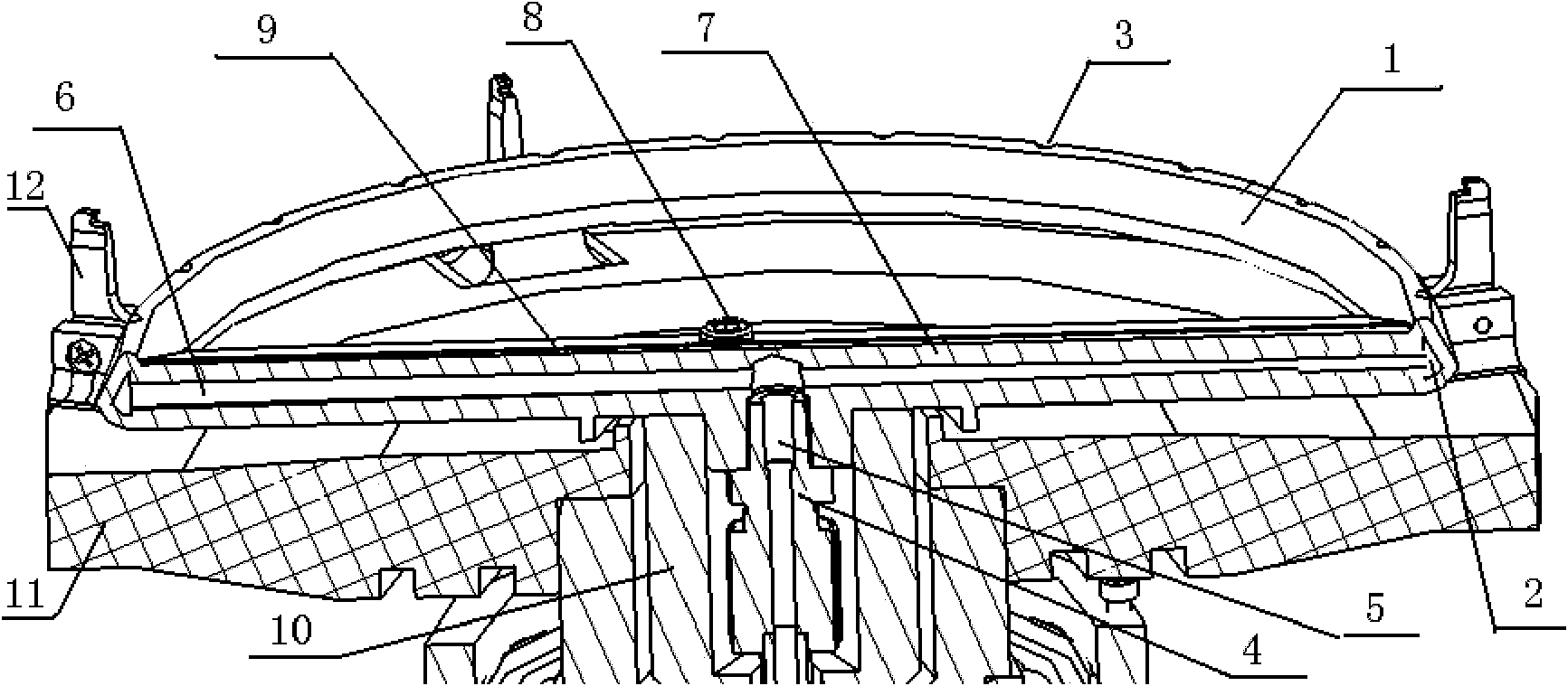
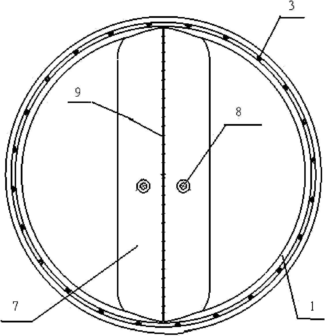
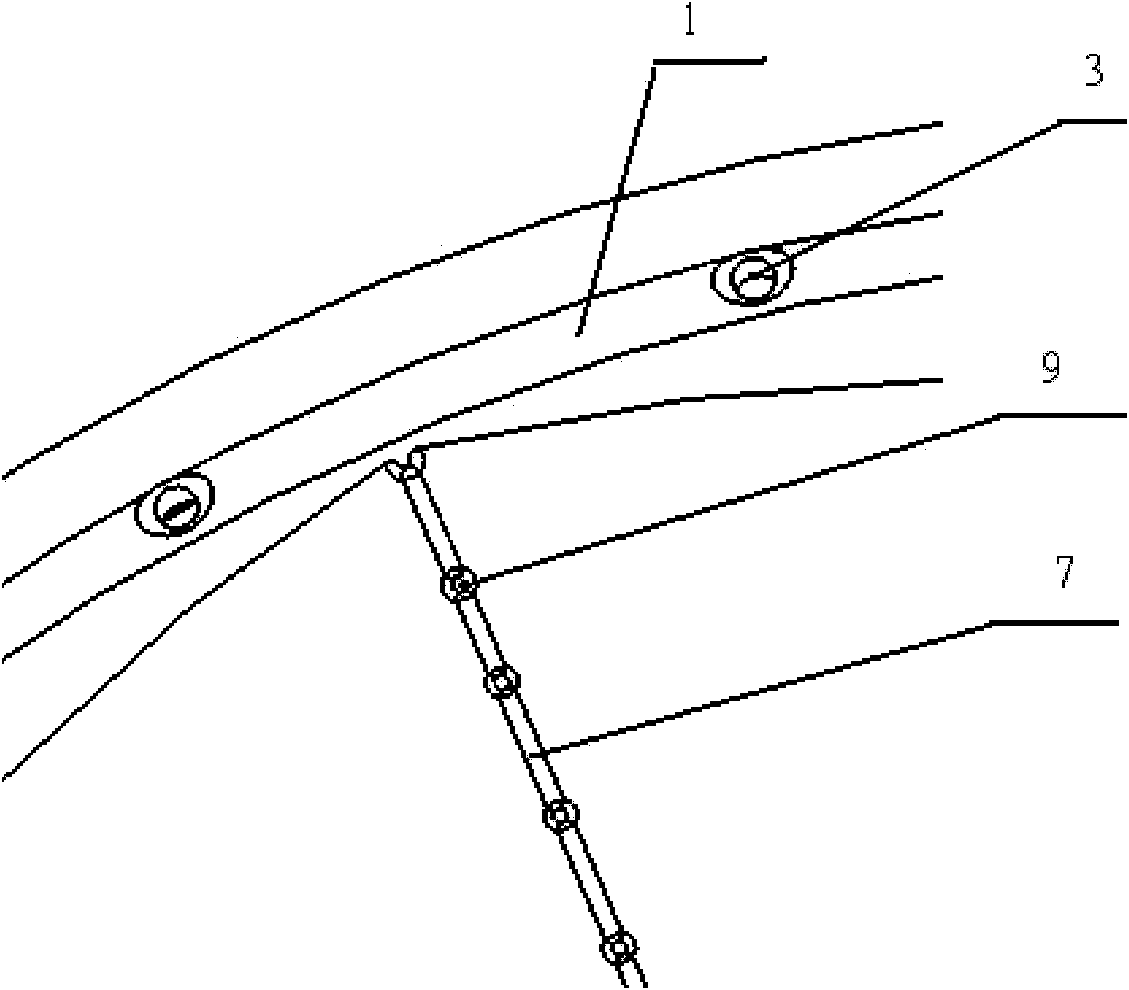
[0023] figure 1 It is a structural schematic diagram of an anti-pollution device according to an embodiment of the present invention, including: a purging unit 1, a gas supply pipeline and a gas supply unit, a vent pipe 2 is arranged in the purging unit 1, and the purging unit The upper end of 1 is provided with a plurality of first air holes 3, and the plurality of first air holes 3 communicate with the ventilation pipe 2 respectively, the ventilation pipe 2 communicates with one end of the air supply pipeline, and the other end of the air supply pipeline communicated with the gas supply unit.

[0024] Preferably, the purging unit 1 is hollow in the shape of a truncated...


PUM


Abstract

The invention discloses a pollution prevention device, relating to the technical field of semiconductor wafer processes. The device comprises a purging unit, a gas supply line and a gas supply unit, wherein a vent pipe is arranged in the purging unit; a plurality of first pores are arranged at the upper end of the purging unit and are respectively communicated with the vent pipe; one end of the gas supply line is communicated with the vent pipe; and the other end of the gas supply line is communicated with the gas supply unit. The device has the following beneficial effects: by arranging the purging unit, the cleaning fluid and cleaning products are prevented from entering into the back of the wafer from the edges of the wafer, thus preventing defects from being formed on the back and edges of the wafer.

Description

technical field [0001] The invention relates to the technical field of semiconductor wafer technology, in particular to an anti-pollution device. Background technique [0002] As the size of the wafer becomes larger and the feature size becomes smaller and smaller, the required cleanliness of the wafer surface becomes more and more stringent. During the wafer cleaning process, chemical reagents and cleaning products easily enter the back of the wafer along the edge of the wafer, causing contamination on the back and edge of the wafer. If this pollution cannot be removed in time, it will cause defects on the back and edge of the wafer, especially in the subsequent high-temperature treatment. During the process, the pollutants on the back and edge will diffuse to the front, seriously affecting the quality of the wafer. However, in the prior art, there is no device that can effectively prevent the contamination of the back and edge of the wafer, so that the quality of the wafer...

Claims


Application Information

Patent Timeline
Patent Type & Authority Applications(China)
IPC IPC(8): B08B3/00H01L21/67
Inventor 刘效岩
Owner BEIJING NAURA MICROELECTRONICS EQUIP CO LTD
Why Eureka
Try Eureka