Filter circuit with coupled bulk acoustic wave resonators with impedance matching adaptation

A filter circuit and resonator technology, applied in the direction of impedance network, electrical components, etc., can solve the problems that hinder the industrial development of this type of structure, the response of the filter does not comply with the telecommunication standard, and it is impossible to imagine the possible combination of impedance matching.

Inactive Publication Date: 2011-12-14
STMICROELECTRONICS SRL
View PDF1 Cites 3 Cited by
  • Summary
  • Abstract
  • Description
  • Claims
  • Application Information

AI Technical Summary

Problems solved by technology

[0030] Therefore, not all possible combinations to achieve impedance matching cannot be conceived
[0031] In addition, and this is an even more unacceptable disadvantage: the known CFR structure requires full control over the manufacturing process of the various layers that make up the component to complete
It has been observed in the laboratory that a low dispersion at the level of the electrode layer, the piezoelectric layer and at the level of the coupling layer leads to an unacceptable shift of the resonant frequency of the upper and lower resonators of the same segment, thus irreversible ground causes the filter response to be non-compliant with the desired telecommunication standard (GSM band, UMTS band, etc.), and thus renders the filter unusable
[0032] Here, there are major limitations to the fabrication process of these structures: fabrication is expensive and it may hinder the industrial development of such structures

Method used


Image

  • Filter circuit with coupled bulk acoustic wave resonators with impedance matching adaptation
  • Filter circuit with coupled bulk acoustic wave resonators with impedance matching adaptation
  • Filter circuit with coupled bulk acoustic wave resonators with impedance matching adaptation

Examples


Embodiment Construction

[0073] The filtering circuit to be described is particularly suitable for the manufacture of RF filtering circuits intended for mobile telephones such as GSM (Global System for Mobile Communications) or WCDMA (Wideband Code Division Multiple Access).

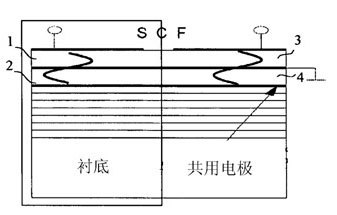
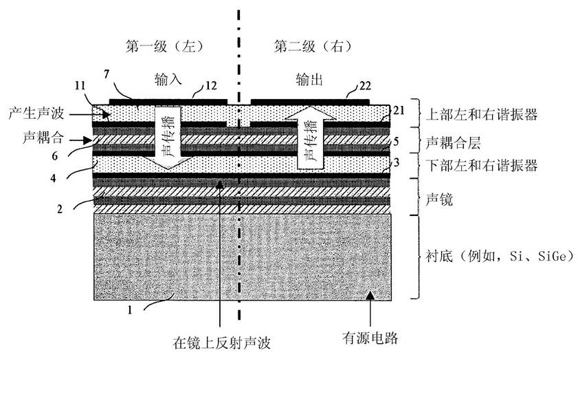
[0074] The circuit according to the invention has a CRF-type architecture comprising a stack of acoustic resonators mounted on a Bragg mirror or membrane. It is reminded that an acoustic mirror comprises a stack of layers with different acoustic impedances, the thickness of which layers is optimized. The alternation of two distinct layers performs the function of reflection of sound waves, one of which exhibits high acoustic impedance and the other exhibits low acoustic impedance.

[0075] see Figure 4A , describing the fabrication of a filter circuit with coupled resonators according to the invention.

[0076] The filter circuit is made from a silicon type substrate 100 built in silicon (Si), gallium arsenide (GaAs), glass o...


PUM


Abstract

The invention provides a filter circuit with coupled resonators comprising: a substrate (100); an acoustic mirror (101) or membrane intended to act as a mechanical support for the acoustic resonators and to isolate these resonators from said substrate; First section (left) comprising an upper resonator (120) and a lower resonator (110) coupled to each other by means of at least one acoustic coupling layer (130), said upper and lower resonators constituting the first section ( A1); a second section (right) comprising an upper resonator (220) and a lower resonator (210) coupled to each other by means of at least one acoustic coupling layer (130), the upper part of the second section and the lower resonator constitute a second section (A2); and a metal via implementing an interstage connection between said lower resonator of one section and said upper resonator of the other section.

Description

Technical field [0001] The invention is an integrated electronic circuit and micro -system in the invention of the body sound wave resonator (BAW). Background technique [0002] The attention of the use of sound resonator is growing with the development of telecommunications, and especially with mobile phones that need to be miniaturized and effective filter circuits.The use of the sound resonator enables high -quality factors in the filter circuit. [0003] Over the past few years, because of its integrated simplicity that its internal quality and SAW (surface sound wave) type resonator cannot provide, the BAW (body sound wave resonator) type sound resonator has produced specific attention to manufacture RF filter circuits. [0004] In addition to its integration in semiconductor circuits, the BAW integrated circuit is particularly concerned due to the multiple combination possibilities provided by the manufacturing complex filter circuit. [0005] The first combination of the s...

Claims


Application Information

Patent Timeline
Patent Type & Authority Applications(China)
IPC IPC(8): H03H9/58
CPCH03H9/584H03H9/588H03H9/0095H03H9/589H03H9/60Y10T29/42
Inventor 琼-弗兰斯瓦·卡朋蒂埃皮埃尔·巴尔亚历山大·沃拉捷
Owner STMICROELECTRONICS SRL
Why Eureka
Try Eureka