Novel double-frequency narrow-band bandpass filter
A filter and a new type of technology, applied in waveguide-type devices, electrical components, circuits, etc., can solve problems such as increased cost, occupation, and the filter cannot meet the needs of wireless communication systems, achieve good harmonic suppression characteristics, and reduce insertion loss. Effect
- Summary
- Abstract
- Description
- Claims
- Application Information
AI Technical Summary
Problems solved by technology
Method used
Image
Examples
Embodiment 1
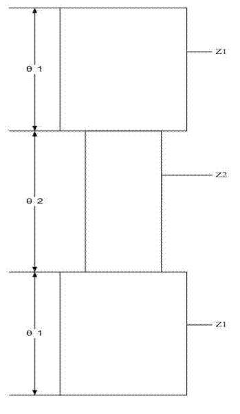
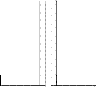
[0032] Embodiment one: see Image 6 , the novel dual-band narrowband bandpass filter comprises a three-layer structure: a metal microstrip line on the front, a dielectric plate layer in the middle and input and output ports, and a metal coating on the back of the dielectric plate. The metal microstrip line structure is : A resonator composed of a low-impedance line and a step impedance line connected to it, and a new resonator composed of a quarter-wavelength uniform impedance line and a feeder connected to a rectangular short microstrip line; since the resonator structure is Symmetrical, so it can be analyzed by odd and even mode theory; the input and output ports of the feeder are on the same horizontal line.
Embodiment 2
[0033] Embodiment 2: This embodiment is basically the same as Embodiment 1, and the special feature is: the step impedance line is formed by connecting a short impedance line (11) at the end of two parallel coupling lines (7), realizing a new coupling. The rectangular short microstrip line (9) is located at the corner where the quarter-wavelength uniform impedance line (8) connects to the feeder line (12), thereby achieving excellent harmonic suppression characteristics. The dielectric plate layer (5) is a dielectric constant =10.2 of the dielectric board, the thickness of the dielectric board h =0.635mm.
Embodiment 3
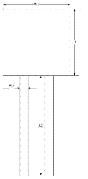
[0034] Embodiment three: this embodiment is basically the same as embodiment two, and the special features are: Image 6 It is a structural schematic diagram of the present embodiment. Through design, simulation and optimization, the specific dimensions of the microstrip ultra-narrowband bandpass filter are finally determined as follows:
[0035] L1=7.3mm, L2=10.0mm, L3=8.4mm, L4=0.8mm
[0036] W1=6.0mm, W2=0.6mm, W3=0.6mm, W4=1.1mm
[0037] G=0.2mm, D=0.2mm,
[0038] Based on the above method, a microstrip filter with a center frequency of 2.62GHz / 5.98GHz and a relative bandwidth of about 6% is designed, and is simulated and debugged by the electromagnetic simulation software Sonnet.
[0039] Figure 7 The frequency response simulation results of a dual-band filter implemented with a conventional structure are shown.
[0040] Figure 8 The simulated structure of the microstrip filter is shown, and the simulated results show that the present invention has great advantages...
PUM
| Property | Measurement | Unit |
|---|---|---|
| Thickness | aaaaa | aaaaa |
Abstract
Description
Claims
Application Information
 - Generate Ideas
- Intellectual Property
- Life Sciences
- Materials
- Tech Scout
- Unparalleled Data Quality
- Higher Quality Content
- 60% Fewer Hallucinations
Browse by: Latest US Patents, China's latest patents, Technical Efficacy Thesaurus, Application Domain, Technology Topic, Popular Technical Reports.
© 2025 PatSnap. All rights reserved.Legal|Privacy policy|Modern Slavery Act Transparency Statement|Sitemap|About US| Contact US: help@patsnap.com


