


Quick Research
Generate reliable direction feasibility study reports for your R&D in just a few steps.

Technical Q&A
Discover and master advanced knowledge NOW. Basics, ideas, possibilities, all at once.

Find Solutions
As an expert in R&D theories, this can generate solutions to your technical problems instantly.

Evaluate Feasibility
Analyze your overall solution with one click, know your potential R&D risks in advance.

Monitor Landscape
Get weekly tech updates, stay abreast of the latest tech innovations and key insights.
LED preparation method to improve light extraction efficiency
A technology of light extraction efficiency and light-emitting layer, applied in the direction of electrical components, circuits, semiconductor devices, etc., can solve problems such as difficult contact and reflection effect, achieve the effect of improving light extraction efficiency and yield, and solving poor adhesion
- Summary
- Abstract
- Description
- Claims
- Application Information
AI Technical Summary
Problems solved by technology
Method used
Image

Examples
preparation example Construction
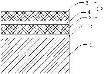
[0055] The present invention proposes a LED preparation method for improving light extraction efficiency, which includes:
[0056] In step a, the buffer layer, n-GaN, light-emitting layer, and p-GaN epitaxial film are grown successively on the sapphire substrate, and then the transparent conductive layer is evaporated and alloyed to grow SiO 2 The protective layer;
[0057] Step b apply viscose to SiO 2 on the protective layer and cured together with the temporary support substrate;
[0058] Step c is to perform laser lift-off of the sapphire substrate;
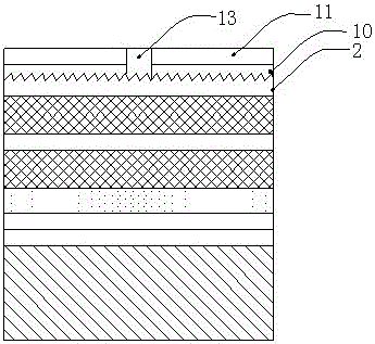
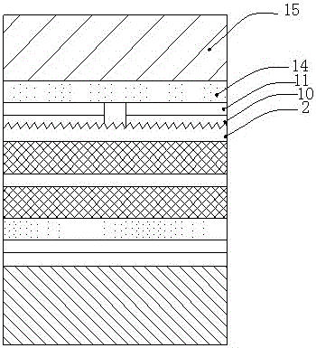
[0059] Step d roughens the N surface of the peeled epitaxial film;
[0060] In step e, a transparent, curable adhesive material layer is made on the N surface of the epitaxial film, and the adhesive material layer is cured;
[0061]In step f, prepare a reflective layer, and perform high-temperature curing together with the above-mentioned adhesive material layer;
[0062] In step g, an electrode-shaped electrode groove i...
Embodiment 3
[0073] Embodiment three of the present invention. The steps of this example are basically the same as those of Example 2. Compared with the second embodiment, the temporary support substrate of this example is made of sapphire. Embodiment three is briefly described as follows:
[0074] After the buffer layer, n-GaN, light-emitting layer, p-GaN and other thin films are grown sequentially on the sapphire substrate by MOCVD, ITO is evaporated and treated with a 500-degree alloy. Apply the viscose to the SiO 2 On the protected ITO layer, and bonded with the temporary support sapphire substrate, cured at 100 degrees for 60 minutes, Kr laser, power 500mW, laser peeling off the sapphire surface. After the sapphire is peeled off, the gallium nitride surface is cleaned and roughened with an alkaline solution (KOH solution) at 80 degrees; the water glass is coated on the gallium nitride roughened surface, and then cured at 80 degrees for 15 minutes. The thickness of the transparent ...
PUM
| Property | Measurement | Unit |
|---|---|---|
| thickness | aaaaa | aaaaa |
| thickness | aaaaa | aaaaa |
Abstract
Description
Claims
Application Information
 - R&D Engineer
- R&D Manager
- IP Professional
- Industry Leading Data Capabilities
- Powerful AI technology
- Patent DNA Extraction
Browse by: Latest US Patents, China's latest patents, Technical Efficacy Thesaurus, Application Domain, Technology Topic, Popular Technical Reports.
© 2024 PatSnap. All rights reserved.Legal|Privacy policy|Modern Slavery Act Transparency Statement|Sitemap|About US| Contact US: help@patsnap.com