Substrate for display panel, and display panel
A technology for display panels and substrates, which is applied in the directions of optics, instruments, electrical components, etc., and can solve problems such as interlayer insulating films that cannot be prevented
- Summary
- Abstract
- Description
- Claims
- Application Information
AI Technical Summary
Problems solved by technology
Method used
Image
Examples
Embodiment Construction
[0056] Hereinafter, various embodiments of the present invention will be described in detail with reference to the drawings. The substrate for a display panel of each embodiment of the present invention is a TFT array substrate suitable for an active matrix type liquid crystal display panel.
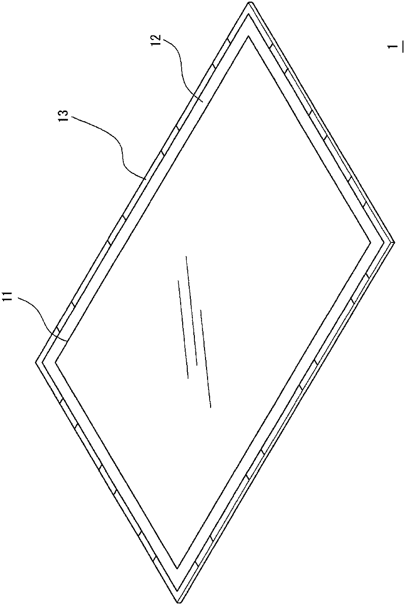
[0057] figure 1 It is an external perspective view schematically showing the schematic structure of the display panel substrate 1 according to the embodiment of the present invention. Such as figure 1 As shown, in the display panel substrate 1 of the embodiment of the present invention, a display area (also referred to as an active area) 11 is provided. Outside the display area 11, a panel frame area 12 is provided around the display area 11.
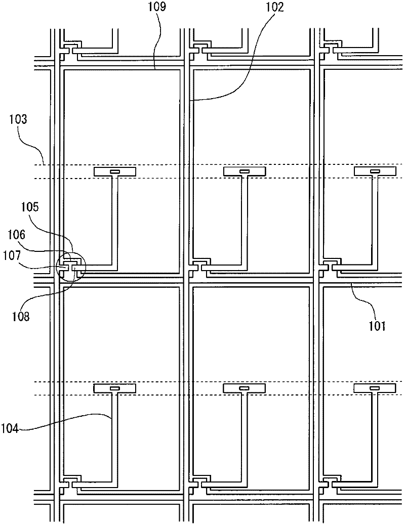
[0058] figure 2 It is a plan view schematically showing the structure of pixels, wirings, and the like provided in the display area 11. Such as figure 2 As shown, a plurality of pixels are arranged in a matrix in the display area 11. Each pixel ...
PUM
| Property | Measurement | Unit |
|---|---|---|
| thickness | aaaaa | aaaaa |
| thickness | aaaaa | aaaaa |
| thickness | aaaaa | aaaaa |
Abstract
Description
Claims
Application Information
 - R&D
- Intellectual Property
- Life Sciences
- Materials
- Tech Scout
- Unparalleled Data Quality
- Higher Quality Content
- 60% Fewer Hallucinations
Browse by: Latest US Patents, China's latest patents, Technical Efficacy Thesaurus, Application Domain, Technology Topic, Popular Technical Reports.
© 2025 PatSnap. All rights reserved.Legal|Privacy policy|Modern Slavery Act Transparency Statement|Sitemap|About US| Contact US: help@patsnap.com


