
White-light organic luminescent device and manufacturing method thereof

An electroluminescent device, organic technology, applied in chemical instruments and methods, semiconductor/solid-state device manufacturing, luminescent materials, etc., can solve the problems of unsuitability for preparation, weakening of light intensity, etc. Effect

Inactive Publication Date: 2011-10-12
UNIV OF ELECTRONICS SCI & TECH OF CHINA
View PDF2 Cites 15 Cited by
  • Summary
  • Abstract
  • Description
  • Claims
  • Application Information

AI Technical Summary

Problems solved by technology

The thickness of the color conversion layer is generally larger than the thickness of the organic functional layer (less than 100nm) in the organic electroluminescent device. In addition, the organic light-emitting material usually weakens the light intensity due to molecular aggregation, that is, it has a concentration quenching effect, so it is not suitable for preparation. Organic Electroluminescent Devices Based on Color Conversion Systems

Method used


Image

  • White-light organic luminescent device and manufacturing method thereof
  • White-light organic luminescent device and manufacturing method thereof
  • White-light organic luminescent device and manufacturing method thereof

Examples


Embodiment 1

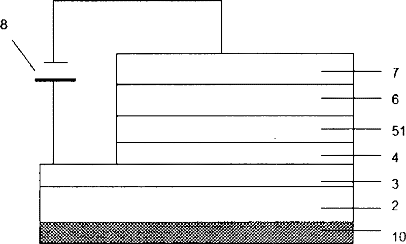
[0053] Such as figure 1 As shown, the color conversion layer 10 in the device structure is a kind of aggregation-induced luminescence yellow light material 1DPAFO, the hole transport material is NPB, the electron transport material is Bphen, the host in the blue light emitting layer 51 is MCP, the guest is FIr6, and the cathode The layer is a Mg:Ag alloy. The entire device structure is described as:

[0054] Yellow color conversion layer 1DPAFO(150nm) / glass substrate / ITO / NPB(40nm) / MCP:8%FIr6(20nm) / Bphen(40nm) / Mg:Ag(200nm)

[0055] The preparation method is as follows:

[0056] ①Use detergent, ethanol solution and deionized water to ultrasonically clean the transparent conductive substrate ITO glass, and dry it with dry nitrogen after cleaning. The ITO film on the glass substrate is used as the anode layer of the device, the square resistance of the ITO film is 10Ω / sq, and the film thickness is 180nm;

[0057] ② Use chloroform as a solvent to configure the solution of the c...

Embodiment 2

[0065] Such as figure 1 As shown, the color conversion layer 10 in the device structure is a kind of aggregation-induced luminescent yellow light material 1DPAFO, the hole transport material is TAPC, the electron transport material is Bphen, the host in the blue light emitting layer 51 is TAPC, and the guest is FIr6, The cathode layer is a Mg:Ag alloy. The entire device structure is described as:

[0066] Yellow color conversion layer 1DPAFO(300nm) / glass substrate / ITO / TAPC(30nm) / TAPC:10%FIr6(30nm) / Bphen(40nm) / Mg:Ag(200nm)

[0067] The preparation process is similar to Example 1.

Embodiment 3

[0069] Such as figure 1 As shown, the color conversion layer 10 in the device structure is a kind of aggregation-induced luminescence yellow light material 2DPAFO, the hole transport material is TAPC, the electron transport material is 3TPYMB, the host in the blue light emitting layer is TBADN, and the guest is DSA-Ph , the cathode layer is Mg:Ag alloy. The entire device structure is described as:

[0070] Yellow color conversion layer 2DPAFO(800nm) / glass substrate / ITO / TAPC(50nm) / TBADN:15%DSA-Ph(20nm) / 3TPYMB(40nm) / Mg:Ag(200nm)

[0071] The preparation process is similar to Example 1.


PUM

PropertyMeasurementUnit
thicknessaaaaaaaaaa
thicknessaaaaaaaaaa

Abstract

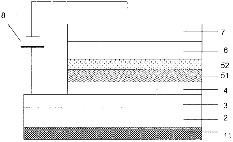
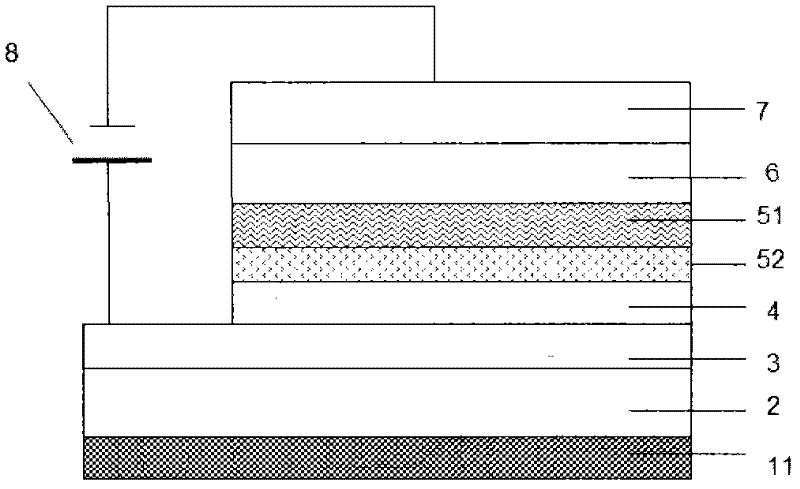
The invention discloses a white-light organic electroluminescent device, which comprises a color conversion layer, a conductive substrate or substrate, a first electrode layer, an organic functional layer and a second electrode layer from bottom to top, wherein the organic functional layer comprises a hole transport layer, a luminous layer and an electron transport layer. The white-light organic electroluminescent device is characterized in that: the luminous layer is a blue-light luminous layer or a green-light luminous layer or a blue-light and green-light co-doped luminous layer; the colorconversion layer is made of a gathering induction luminous material and is used for emitting yellow light or red light based on a gathering induction luminescent mechanism; the gathering induction luminous material is used for absorbing a part of blue light or green light emitted by the luminous layer and converting the blue light or green light into yellow light or red light for emitting; and white light is formed by mixing three primary colors or complementary colors.

Description

technical field [0001] The invention relates to the field of organic photoelectric technology in electronic components, in particular to a white light organic electroluminescent device and a preparation method thereof. Background technique [0002] Organic light-emitting devices (Organic light-emitting devices, OLEDs) are a new type of photoelectric display and high-efficiency lighting technology. , especially suitable for the requirements of low-carbon environmental protection and green life in today's world, and has been widely used in various fields of daily production and life such as flat panel display, solid-state lighting, transparent display, flexible display and lighting. [0003] There are many ways to prepare white light organic electroluminescent devices, such as co-doping of multiple fluorescent or phosphorescent dyes in one light emitting layer, multi-light emitting layer structure composed of different light emitting colors, stacked structure, white light poly...

Claims


Application Information

Patent Timeline
Patent Type & Authority Applications(China)
IPC IPC(8): H01L51/52H01L51/54H01L51/56C09K11/06
CPCY02B20/00
Inventor 于军胜赵娟张磊蒋亚东
Owner UNIV OF ELECTRONICS SCI & TECH OF CHINA
Learn More