
Active matrix substrate, liquid crystal display panel, liquid crystal display device, method for manufacturing active matrix substrate, method for manufacturing liquid crystal display panel and method for driving liquid crystal display panel

An active matrix and substrate technology, applied in static indicators, nonlinear optics, instruments, etc., can solve the problems of weak orientation restriction and difficulty in changing the orientation of liquid crystals

Inactive Publication Date: 2014-09-17
SHARP KK
View PDF6 Cites 0 Cited by
  • Summary
  • Abstract
  • Description
  • Claims
  • Application Information

AI Technical Summary

Problems solved by technology

According to PSA, even in a pixel structure with a weak orientation restriction force for the purpose of increasing the aperture ratio, etc., the response speed is fast, and it is difficult to change the orientation of the liquid crystal by finger pressing, etc.

Method used


Image

  • Active matrix substrate, liquid crystal display panel, liquid crystal display device, method for manufacturing active matrix substrate, method for manufacturing liquid crystal display panel and method for driving liquid crystal display panel
  • Active matrix substrate, liquid crystal display panel, liquid crystal display device, method for manufacturing active matrix substrate, method for manufacturing liquid crystal display panel and method for driving liquid crystal display panel
  • Active matrix substrate, liquid crystal display panel, liquid crystal display device, method for manufacturing active matrix substrate, method for manufacturing liquid crystal display panel and method for driving liquid crystal display panel

Examples


Embodiment Construction

[0105] (Outline of Liquid Crystal Display Device 1 )

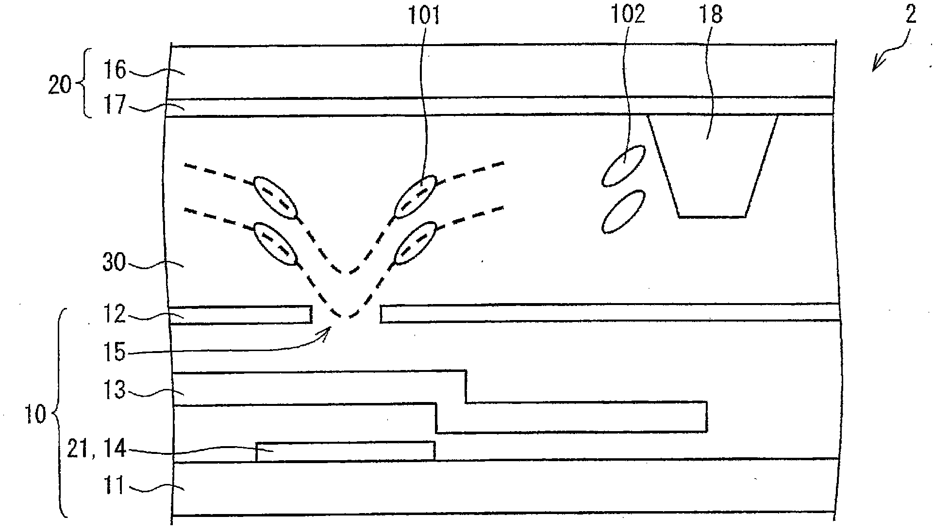
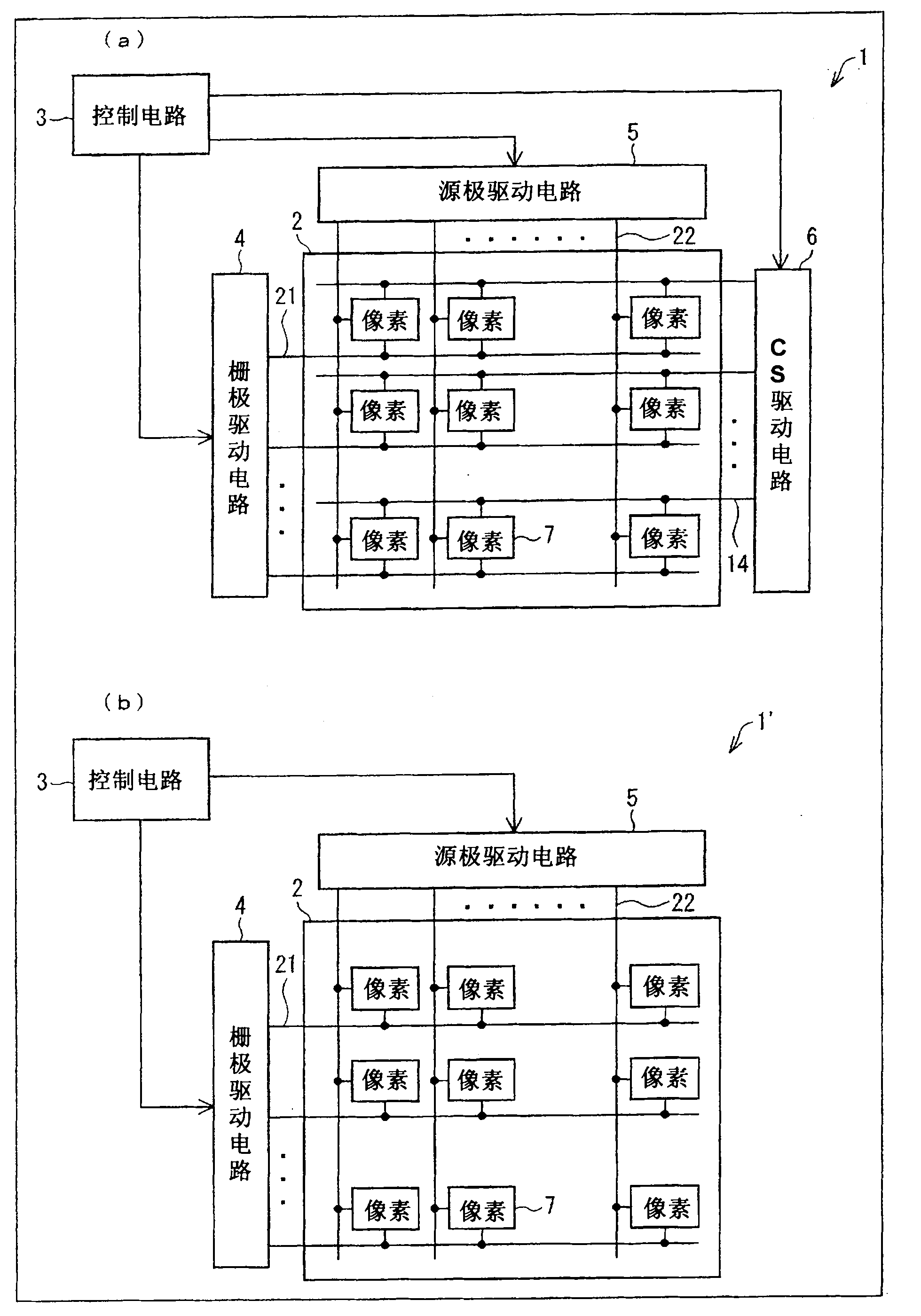
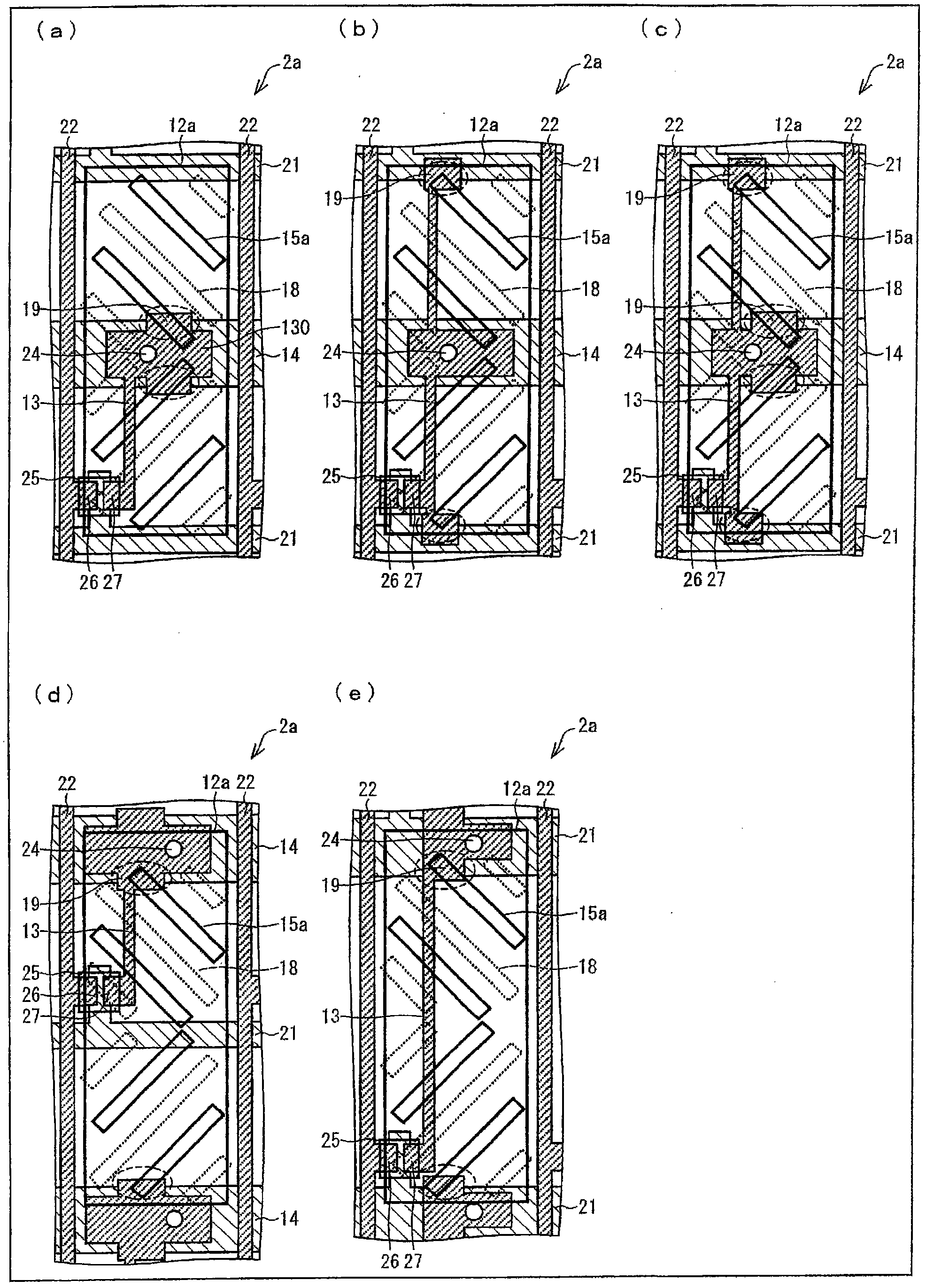
[0106] refer to Figure 1 to Figure 8 The first embodiment of the present invention will be described. First, the outline of the liquid crystal display device 1 in this embodiment will be described. figure 1 It is a cross-sectional view schematically showing the structure of the main part of the liquid crystal display panel 2 according to the present embodiment. in addition, figure 2 is a block diagram showing a schematic configuration of a liquid crystal display device according to this embodiment, figure 2 (a) shows a liquid crystal display device 1 driven using a storage capacitor, figure 2 (b) shows a liquid crystal display device 1' driven without using an auxiliary capacitor.

[0107] Such as figure 2 As shown in (a), the liquid crystal display device 1 according to this embodiment includes a liquid crystal display panel 2, a driving circuit for driving the liquid crystal display panel 2, a control circuit...


PUM


Abstract

The present invention relates to a liquid crystal display panel including a substrate having a structure in which a slit of a pixel electrode intersects a scanning signal line or an auxiliary capacitor line, which can suppress alignment disorder in the liquid crystal display panel and realize high-quality display. The active matrix substrate (10) is provided with a pixel electrode (12) having a slit (15) and an auxiliary capacitor line (14), in a region where the auxiliary capacitor line (14) or the scanning signal line (21) and the slit (15) intersect , between the layer of the pixel electrode (12) and the layer of the auxiliary capacitor line (14) or the scanning signal line (21), a drain electrode is formed so as to cover the auxiliary capacitor line (12) or the scanning signal line (21) at least any one of the line (13) or the data signal line (22).

Description

technical field [0001] The invention relates to an active matrix substrate for controlling the orientation of liquid crystal molecules and displaying video, a liquid crystal display panel, a liquid crystal display device, a method for manufacturing an active matrix substrate, and a method for manufacturing a liquid crystal display panel, and in particular relates to a method for manufacturing a liquid crystal display panel utilizing a PSA (Polymer Sustained Alignment, active matrix substrate, liquid crystal display panel, liquid crystal display device, active matrix substrate manufacturing method, liquid crystal display panel manufacturing method and liquid crystal display panel driving method manufactured by the manufacturing method of polymer stable orientation) treatment. Background technique [0002] In recent years, along with the popularization of information equipment, there has been an increasing demand for higher performance of display panels (liquid crystal display ...

Claims


Application Information

Patent Timeline
Patent Type & Authority Patents(China)
IPC IPC(8): G02F1/1343G02F1/1368
CPCG02F2001/133769G02F2203/62G02F2201/128G02F1/133788G02F2001/134345G02F2201/40G09G3/3655G02F2001/133715G02F2001/13629G02F1/13624G02F1/1337G09G2330/10G02F2001/134372G02F1/133707G09G3/3637G02F1/133715G02F1/133769G02F1/134345G02F1/134372G02F1/13629
Inventor 堀内智山田崇晴久田祐子伊藤了基
Owner SHARP KK
Learn More