High-wavelength antimonide semiconductor laser structure

A laser and antimonide technology, applied in semiconductor lasers, lasers, laser parts, etc., to reduce optical mode loss, improve structural efficiency, and improve performance

Inactive Publication Date: 2011-10-05
CHANGCHUN UNIV OF SCI & TECH
View PDF3 Cites 5 Cited by
  • Summary
  • Abstract
  • Description
  • Claims
  • Application Information

AI Technical Summary

Problems solved by technology

[0004] The present invention aims at the problems and shortcomings of the antimonide excitation increasing with the increase of the wavelength, and the power and efficiency become worse, and proposes a long-wavelength antimonide semiconductor laser structure, which reduces the problem of laser power and efficiency deterioration caused by free carrier absorption and the like. question

Method used


Image

  • High-wavelength antimonide semiconductor laser structure

Examples


Embodiment Construction

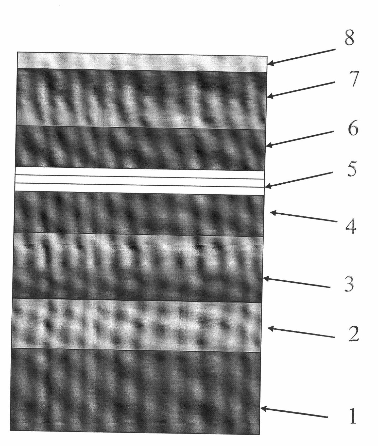
[0008] Such as figure 1 As shown, a long-wavelength antimonide semiconductor laser structure includes:

[0009] The substrate 1 has a (100) orientation and a Te doping concentration of 1 to 2×10 18 cm -3 GaSb crystal material.

[0010] GaSb buffer layer 2, growth temperature 560°C, Te doping concentration 2×10 18 cm -3 , thickness 1 μm.

[0011] Al x Ga 1-x Sb lower confinement layer 3, grown at a temperature range of 540-560°C, doped with Te at a concentration of 1×10 19 cm -3 -3×10 18 cm -3 , growing 1.2 μm. Using variable Al composition and segmented-gradient doping design and growth, combined with figure 1 It shows that from the direction of layer 3 to layer 4, the Al composition x changes from 0.9 to 0.75 at the first growth thickness of 0.7 μm. The doping concentration is changed from 1×10 19 cm -3 Change to 5×10 18 cm -3 . For the thickness of 0.5 μm grown next, the Al composition x changes from 0.75 to 0.45, and the doping concentration changes from 5...


PUM


Abstract

The invention discloses a high-wavelength antimonide semiconductor laser structure, which belongs to the field of epitaxial structures made from novel materials for semiconductor lasers and aims at the problems and shortcomings that the power, efficiency and the like of an antimonide laser are lowered along with the increasing of wavelengths. The laser structure can alleviate the problem that the power and efficiency of the laser are lowered due to free charge carrier absorption and the like, has the characteristics of low optical mode loss, strong cavity restrictions, low internal loss, high quantum well laser structure efficiency and the like, and can improve the performance of the antimonide laser such as the power, the efficiency and the like.

Description

technical field [0001] The invention relates to the technical field of semiconductor laser materials, and belongs to the field of epitaxial structure of new semiconductor laser materials. technical background [0002] Antimonide lasers tend to develop towards long wavelength, high power and high efficiency. In InGaAsSb / AlGaAsSb quantum well lasers in the mid-wave infrared band above 3 μm, free carrier absorption has become a serious problem, resulting in increased internal loss, causing the threshold current, quantum efficiency, and electro-optical conversion efficiency of the device to increase with wavelength. And get worse. For example, the quantum efficiency (30%) of the 2.8 μm laser developed by the Sarnoff Research Center is only about half of the quantum efficiency (60%) of the 2.5 μm laser. The electro-optical conversion efficiency (PCE) of the 3.5 μm laser developed by SUNY Stony Brook is 8%, which is only about 45% of the efficiency of the 2.4 μm (17.5%) laser. ...

Claims


Application Information

Patent Timeline
Patent Type & Authority Applications(China)
IPC IPC(8): H01S5/343
Inventor 李占国尤明慧刘国军高欣李林李辉芦鹏王勇邹永刚乔忠良李梅曲轶薄报学
Owner CHANGCHUN UNIV OF SCI & TECH
Why Eureka
Try Eureka