
Deep trench filling method of superstructure

A filling method and deep trench technology, which is applied in the direction of electrical components, semiconductor/solid-state device manufacturing, circuits, etc., can solve the problems of leakage, reduce the electrical performance and mechanical performance of devices, and achieve the elimination of gaps, avoid leakage phenomenon, and meet the tolerance The effect of high voltage electrical requirements

Inactive Publication Date: 2011-09-14
ADVANCED SEMICON MFG CO LTD
View PDF2 Cites 2 Cited by
  • Summary
  • Abstract
  • Description
  • Claims
  • Application Information

AI Technical Summary

Problems solved by technology

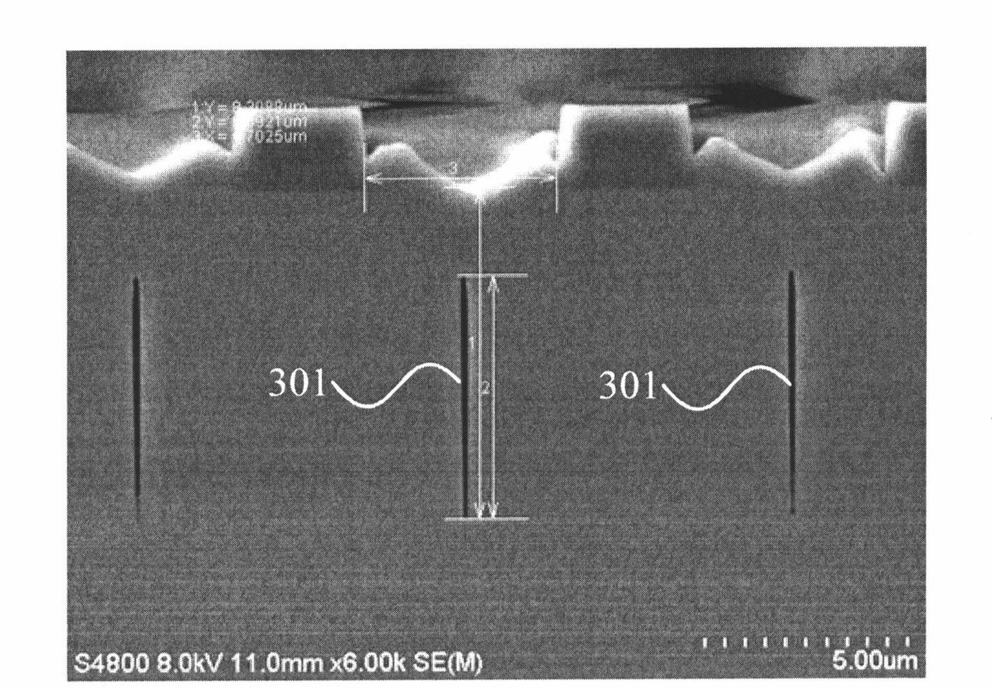
As shown in the figure, the long and narrow slit 301 in the deep trench will cause leakage when the Cool MOS device is working, thereby reducing the electrical and mechanical properties of the device

Method used

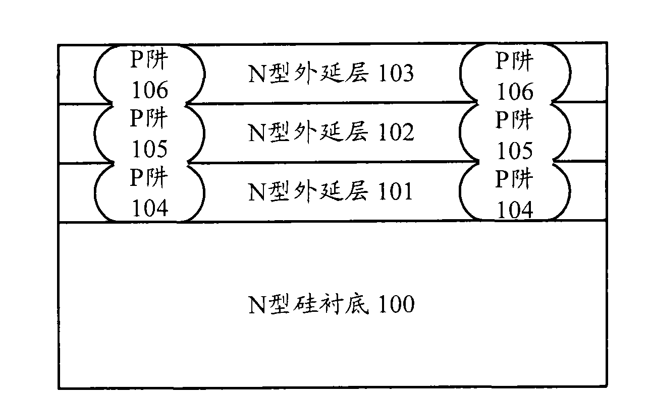
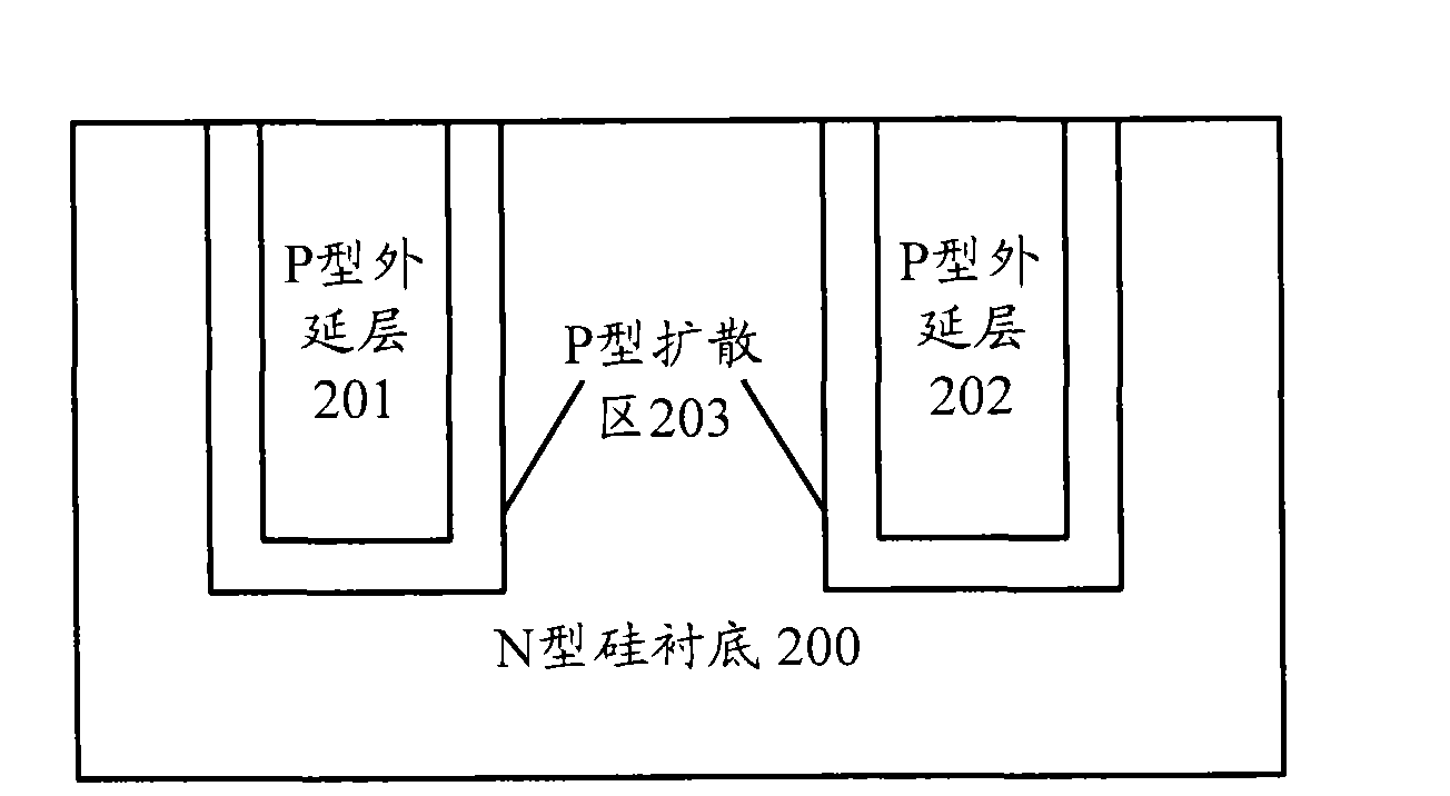

Image

  • Deep trench filling method of superstructure
  • Deep trench filling method of superstructure
  • Deep trench filling method of superstructure

Examples


Embodiment Construction

[0032] The present invention will be further described below in conjunction with specific embodiments and accompanying drawings, but the protection scope of the present invention should not be limited thereby.

[0033] Figure 4 It is a flowchart of a deep trench filling method for a super junction structure according to an embodiment of the present invention. As shown in the figure, the manufacturing method starts at step S401. The method may include: performing step S401, providing a deep trench for forming a super junction structure, and the deep trench is located in an N-type epitaxial layer on an N-type semiconductor substrate; performing step S402, growing a P-type epitaxial layer in the deep trench Layer, a gap is left in the middle of the P-type epitaxial layer; perform step S403, deposit an oxide layer in the middle of the P-type epitaxial layer, and fill the deep trench; perform step S404, dry-etch the oxide layer in the deep trench, so that the deep The top of the...


PUM

PropertyMeasurementUnit
Thicknessaaaaaaaaaa
Depthaaaaaaaaaa

Abstract

The invention provides a deep trench filling method of a superstructure. The method comprises the steps of A. providing a deep trench to form the superstructure; B. growing a P-type epitaxial layer in the deep trench; C. depositing an oxidation layer in the middle of the P-type epitaxial layer and filing the deep trench; D. dry etching the oxidation layer in the deep trench to enable the top of the deep trench to be opened; and E. continuing to deposit the oxidation layer in the deep trench and filling the deep trench, wherein the deep trench is positioned in the N-type epitaxial layer on an N-type semiconductor substrate; and a gap is remained in the middle of the P-type epitaxial layer. Through alternately depositing the oxidation layer in the deep trench of the superstructure and etching the oxidation layer at the top of the deep trench to enable the trench opening to be fully opened, the method realizes completely seamless deep trench filling gradually, eliminates the long and narrow gap in the trench, avoids leakage phenomenon, and enables the power MOS device to meet the electrical requirement on high voltage bearing and the mechanical requirement on grinding and packaging a silicon wafer into sheets.

Description

technical field [0001] The invention relates to the technical field of semiconductor manufacturing, in particular, the invention relates to a deep trench filling method of a super junction structure. Background technique [0002] Power MOS devices are widely used in middle and high-end applications due to their high input impedance, low loss, fast switching speed, no secondary breakdown, wide safe operating area, good dynamic performance, easy coupling with the front electrode to achieve large current, and high conversion efficiency. Low power conversion and control field. Although power MOS devices have been amazingly improved in terms of power handling capability, their on-resistance also increases exponentially with the increase of operating voltage in the high-voltage field, making the conduction loss of power MOS devices increase with the withstand voltage increased rapidly. [0003] In order to break the silicon limit of on-resistance, increase withstand voltage, red...

Claims


Application Information

Patent Timeline
IPC IPC(8): H01L21/762
Inventor 陶有飞钱慧
Owner ADVANCED SEMICON MFG CO LTD
Learn More