Mems sensor
A sensor and substrate technology, applied in the field of MEMS sensors, can solve the problems of easy deviation of plane size, deviation of joint strength, reduction of joint area, etc., and achieve the effects of reducing deviation, improving joint strength and stabilizing joint strength
- Summary
- Abstract
- Description
- Claims
- Application Information
AI Technical Summary
Problems solved by technology
Method used
Image

Examples
Embodiment Construction
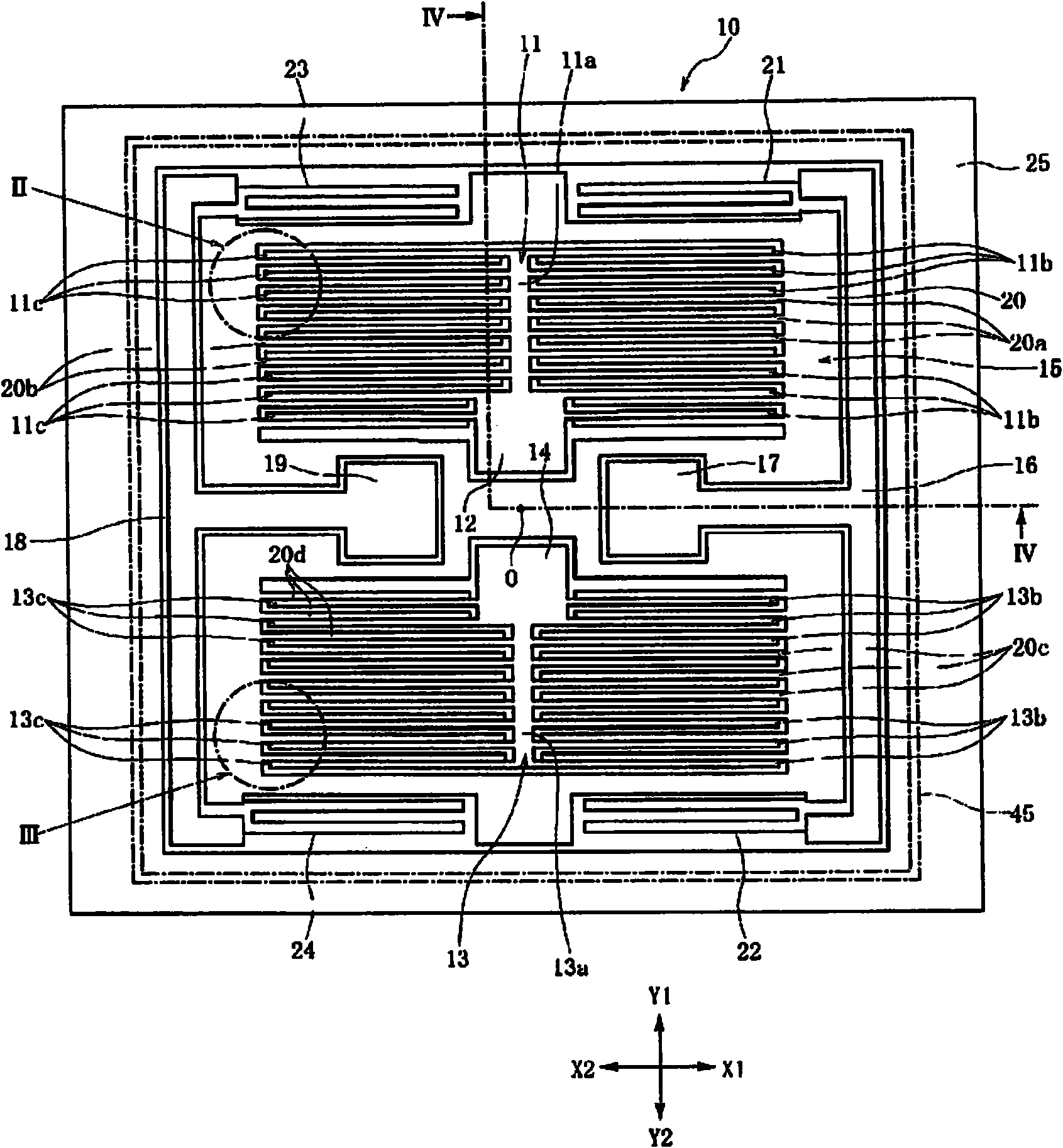
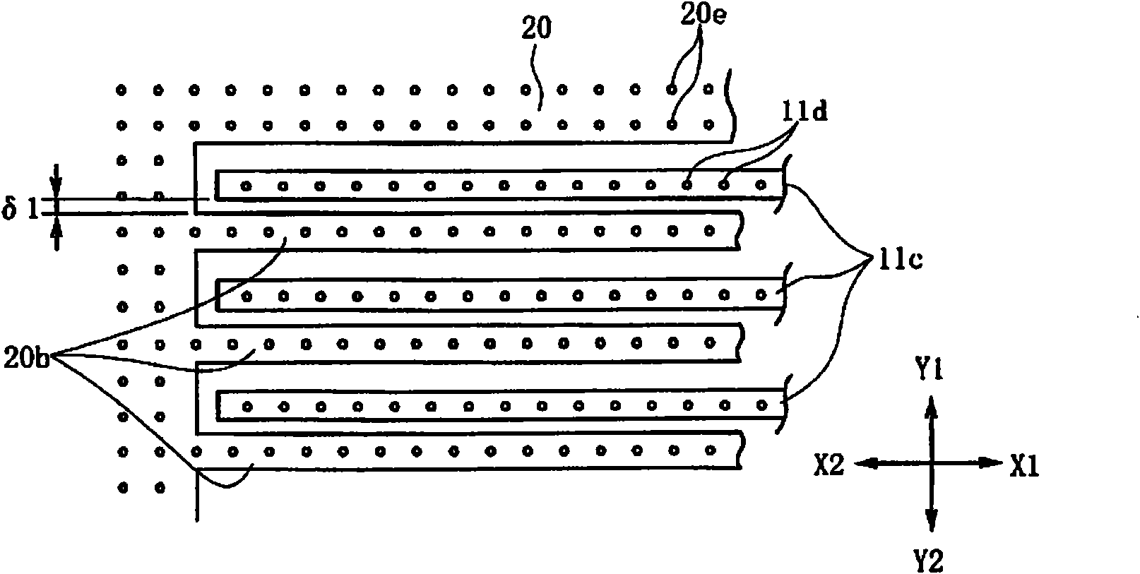
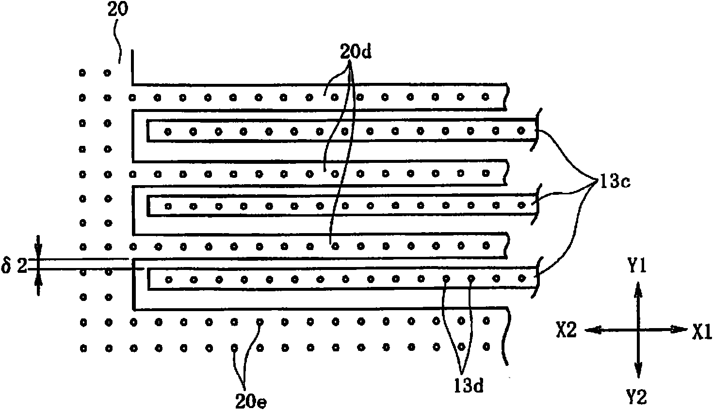
[0068] figure 1 The MEMS sensor showing the embodiment of the present invention is a plan view showing the movable electrode part, the fixed electrode part, and the frame body layer. exist figure 1 In , the illustration of the first substrate and the second substrate is omitted. figure 2 Yes figure 1 Enlarged view of Part II of image 3 It is an enlarged view of Part III. Figure 4 It is a cross-sectional view showing the overall structure of the MEMS sensor, and is equivalent to cutting along line IV-IV figure 1 cross-sectional view. Figure 5 equivalent to Figure 4 An enlarged cross-sectional view of the V portion of . Image 6 With Figure 5 Enlarged cross-sectional views of MEMS sensors of various other embodiments.
[0069] like Figure 4 As shown, the MEMS sensor sandwiches a functional layer 10 between a first substrate 1 and a second substrate 2 . Each part of the first substrate 1 and the functional layer 10 is bonded via the first insulating layers 3...
PUM
 Abstract
Description
Claims
Application Information
 - R&D
- Intellectual Property
- Life Sciences
- Materials
- Tech Scout
- Unparalleled Data Quality
- Higher Quality Content
- 60% Fewer Hallucinations
Browse by: Latest US Patents, China's latest patents, Technical Efficacy Thesaurus, Application Domain, Technology Topic, Popular Technical Reports.
© 2025 PatSnap. All rights reserved.Legal|Privacy policy|Modern Slavery Act Transparency Statement|Sitemap|About US| Contact US: help@patsnap.com