Nitride light-emitting diode capable of enhancing carrier injection efficiency and manufacturing method thereof

A technology of light-emitting diodes and nitrides, which is applied to electrical components, circuits, semiconductor devices, etc., can solve the problems of low injection efficiency of electrons and holes, and achieve the effects of increasing the probability of tunneling, suppressing the tunneling effect, and reducing leakage

Inactive Publication Date: 2012-09-26
SUN YAT SEN UNIV
View PDF3 Cites 1 Cited by
  • Summary
  • Abstract
  • Description
  • Claims
  • Application Information

AI Technical Summary

Problems solved by technology

[0006] The purpose of the present invention is to overcome the defects of low electron and hole injection efficiency in the active layer region of the existing nitride light emitting diode, and provide a nitride light emitting diode that can simultaneously enhance the injection efficiency of electrons and hole carriers

Method used


Image

  • Nitride light-emitting diode capable of enhancing carrier injection efficiency and manufacturing method thereof
  • Nitride light-emitting diode capable of enhancing carrier injection efficiency and manufacturing method thereof
  • Nitride light-emitting diode capable of enhancing carrier injection efficiency and manufacturing method thereof

Examples


Embodiment 1

[0057] 1. If Figure 4 , using ordinary metal oxide vapor deposition (MOCVD) equipment, the substrate material 11 is a sapphire (0001) surface substrate; an initial growth layer 12 with a thickness of 20nm, and a GaN buffer layer 13 with a thickness of 1μm are sequentially grown on the substrate and a Si-doped n-type GaN electron injection layer 14 with a thickness of 2 μm;

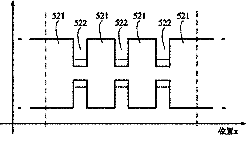
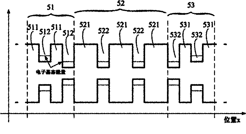
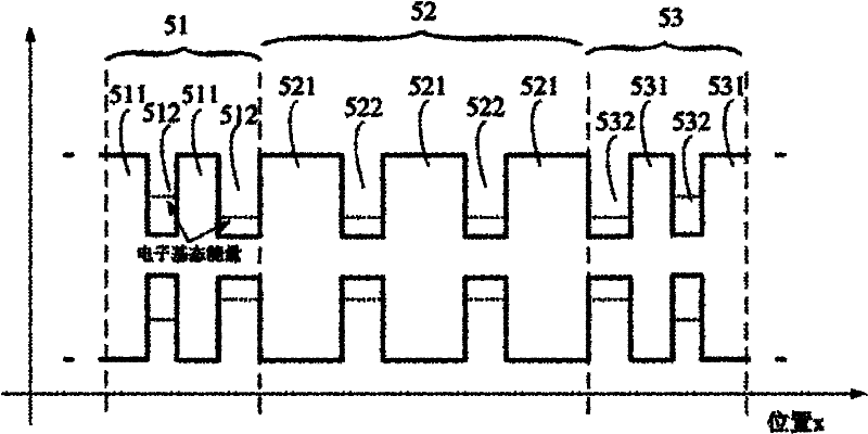
[0058] 2. On the basis of step 1, grow the coupled multi-quantum well active layer 15 through temperature control: sequentially grow 1) electron injection to strengthen the quantum well layer 51, and change the growth temperature of the InGaN quantum well to gradually change the In composition Large, shallow wells with low In composition are close to the n-type electron injection layer; 2) The compound quantum well region 52 in the middle keeps the growth temperature of the InGaN quantum well at a constant value and is equal to the temperature of the last quantum well in the electron-enhanced injection regi...

Embodiment 2

[0063] 1. As in Example 1, common metal oxide vapor deposition (MOCVD) equipment is used, and the substrate material 11 is a sapphire (0001) surface substrate; an initial growth layer 12 with a thickness of 20 nm is sequentially grown on the substrate, and the thickness is a GaN buffer layer 13 of 1 μm and a Si-doped n-type GaN electron injection layer 14 with a thickness of 2 μm;

[0064] 2. On the basis of step 1, grow the coupled multi-quantum well active layer 15 through thickness control: sequentially grow 1) electron injection to strengthen the quantum well layer 51, and change the growth time of the InGaN quantum well to gradually increase the well width. The narrow well is close to the n-type electron injection layer; 2) The compound quantum well region 52 in the middle keeps the growth time of the InGaN quantum well at a constant value and is equal to the time of electron strengthening injection for the last quantum well in the injection region. 3) Hole injection stre...


PUM


Abstract

The invention relates to a nitride light-emitting diode capable of enhancing carrier injection efficiency and a manufacturing method thereof. The nitride light-emitting diode at least comprises an n-type electron injection layer, a coupling multiple-quantum-well structure active layer and a p-type hole injection layer, wherein the coupling multiple-quantum-well structure active layer comprises anelectron injection enhancement quantum well layer, a hole injection enhancement quantum well layer and a composite quantum well region layer, wherein the electron injection enhancement quantum well layer is close to the n-type electron injection layer; the hole injection enhancement quantum well layer is close to the p-type hole injection layer; the composite quantum well region layer is positioned between the electron injection enhancement quantum well layer and the hole injection enhancement quantum well layer; and the barrier width in an electron / hole injection enhancement region layer is less than that of the composite quantum well region layer. The invention also relates to the manufacturing method of the nitride light-emitting diode. The invention has the advantage of respectively and simultaneously enhancing the efficiency of injecting electron and hole carriers into an active region layer in a tunneling way by utilizing the variation distribution of the electronic ground stateenergy of quantum wells positioned in the coupling multiple-quantum well structure active layer, thereby enhancing the light-emitting efficiency of the nitride light-emitting diode.

Description

technical field [0001] The invention belongs to the field of light-emitting diodes, and specifically relates to a nitride light-emitting diode that enhances carrier injection efficiency, and specifically includes a manufacturing method of the diode. Background technique [0002] Light-emitting diode (LED) is an injection electroluminescent device. The tunable range of LED wavelength of GaN-based materials theoretically covers the entire visible light band, so its application fields are very broad. Nitride LED devices based on GaN-based materials are widely used in large-screen full-color display, TV and computer backlight, automotive lighting, road lighting and medical fields. Recently, the application of LEDs in indoor lighting has become more and more common, and it is expected to gradually replace traditional fluorescent lamps as a new generation of lighting sources. Although LED has advantages that traditional lighting sources do not have in terms of energy saving and ...

Claims


Application Information

Patent Timeline
Patent Type & Authority Patents(China)
IPC IPC(8): H01L33/32H01L33/04H01L33/00
Inventor 江灏王钢黄善津
Owner SUN YAT SEN UNIV
Why Eureka
Try Eureka