
Microstrip antenna element with controllable directional diagram

A technology of microstrip antenna and pattern, applied in the direction of antenna, antenna grounding device, electrical components, etc., can solve the problems of changing the maximum point of the antenna array, low antenna efficiency, and high external dimensions.

Inactive Publication Date: 2011-08-03
NANJING UNIV OF SCI & TECH
View PDF1 Cites 13 Cited by
  • Summary
  • Abstract
  • Description
  • Claims
  • Application Information

AI Technical Summary

Problems solved by technology

However, since the microstrip unit pattern is limited by its own structure and working method, it is impossible to change the maximum point of the antenna array by changing the amplitude and phase characteristics of each unit in the array as conveniently as the antenna array.
According to our research, there are currently two methods to realize the control of the unit pattern: (1) By adopting different working modes when designing the antenna, but using this method to control the antenna unit pattern has several shortcomings: 1. The efficiency of the antenna using the high-order mode working mode is not high; 2. The maximum pointing angle is limited, and only the change of a fixed angle can be realized; 3. The size of the antenna unit is changed, and it is often necessary to increase the size of the antenna unit in order to realize the change of the working mode at a fixed frequency Or reduce the size of the antenna, which will have high requirements for the external dimensions; 4. Increase the difficulty of design
(2) By changing the size of the dielectric plate of the microstrip antenna, the unit pattern is controlled by surface wave radiation, but this method is at the cost of volume. If it is for some compact structures, this method is not applicable

Method used


Image

  • Microstrip antenna element with controllable directional diagram
  • Microstrip antenna element with controllable directional diagram
  • Microstrip antenna element with controllable directional diagram

Examples


Embodiment 1

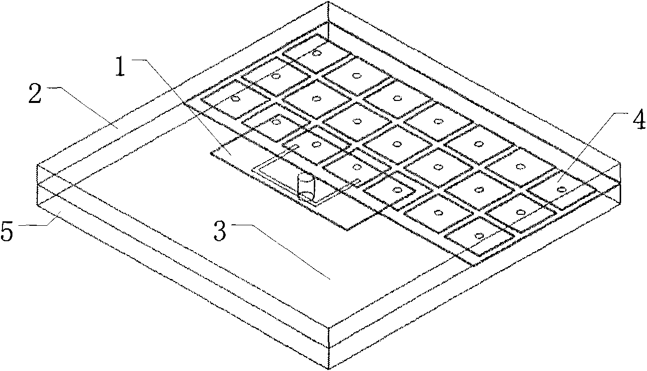
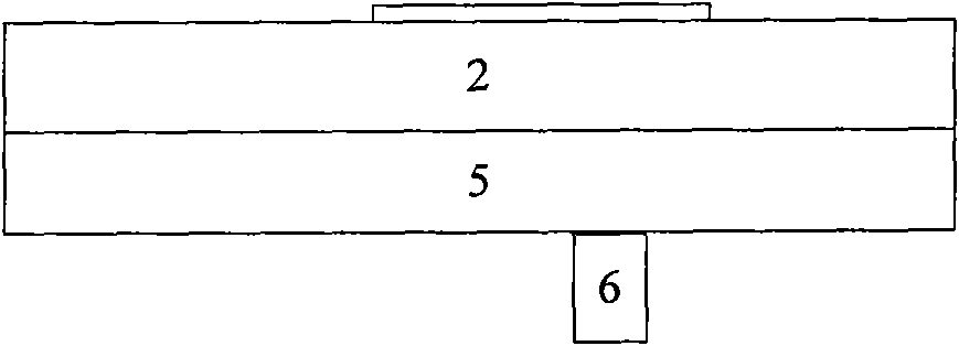
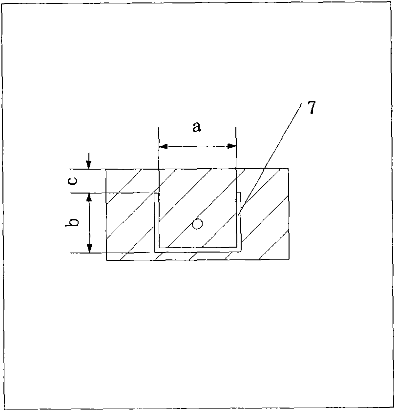
[0022] to combine figure 2 Or 6, a microstrip antenna unit with a controllable pattern, using double-layered dielectric boards, the area of ​​the two dielectric boards is 50mm×50mm, the surface of the first layer of dielectric board 2 is etched with the microstrip antenna unit 1, and its The size is 21.6mm×11.4mm; the microstrip antenna unit 1 has a U-shaped slit 7 etched on the first layer of dielectric substrate 2, the dielectric constant of the first layer of dielectric substrate 2 is 2.7, the thickness is 3.5mm, and the U-shaped slit The width of the U-shaped slots is 0.6mm, the distance between the U-shaped slots parallel to each other is 10mm, and their length is 15.5mm. Feed. The upper surface of the second dielectric board 5 is composed of a metal ground 3 and an EBG metal patch 4, the lower surface of the second dielectric board 5 is a complete metal ground 9, and the EBG metal patch 4 passes through the second metal via hole 8. The layer dielectric board 5 is conn...

Embodiment 2

[0024] to combine figure 2Or 7, further improvement on the basis of the embodiment can obtain a microstrip antenna unit with a controllable pattern, using double-layered dielectric boards, the area of ​​the two-layer dielectric boards is 50mm×50mm, and the first layer of dielectric boards 2 Surface etching microstrip antenna unit 1, the size of which is 21.6mm×11.4mm; microstrip antenna unit 1 has a U-shaped slit 7 etched on the first layer of dielectric substrate 2, and the dielectric constant of the first layer of dielectric substrate 2 is 2.7, the thickness is 3.5mm, the width of the U-shaped slot is 0.6mm, the distance between the U-shaped slots parallel to each other is 10mm, and their length is 15.5mm, the distance between the upper edge of the U-shaped slot and the upper edge of the microstrip antenna unit 1 is 3.1mm, and fed through the coaxial probe 6. The upper surface of the second dielectric board 5 is composed of a metal ground 3 and an EBG metal patch 4, the lo...

Embodiment 3

[0026] combine figure 2 Or 8, improving Embodiment 2 to obtain a microstrip antenna unit with a controllable pattern, using double-layer dielectric boards, the area of ​​the two-layer dielectric boards is 50mm×50mm, and the surface of the first layer of dielectric board 2 Etching the microstrip antenna unit 1, the size of which is 21.6mm×11.4mm; the microstrip antenna unit 1 has a U-shaped slit 7 etched on the first layer of dielectric substrate 2, the dielectric constant of the first layer of dielectric substrate 2 is 2.7, The thickness is 3.5mm, the width of the U-shaped slot is 0.6mm, the distance between the U-shaped slots parallel to each other is 10mm, and their length is 15.5mm, and the distance between the upper edge of the U-shaped slot and the upper edge of the microstrip antenna unit 1 is 3.1mm , and fed through the coaxial probe 6. The upper surface of the second dielectric board 5 is composed of a metal ground 3 and an EBG metal patch 4, the lower surface of the...


PUM

PropertyMeasurementUnit
thicknessaaaaaaaaaa
widthaaaaaaaaaa
lengthaaaaaaaaaa

Abstract

The invention relates to a microstrip antenna element with a controllable directional diagram. Dielectric slabs which are stacked up in two layers are used; the microstrip antenna element is etched on the surface of a first dielectric slab; the upper surface of a second dielectric slab consists of a metal ground and EBG (electromagnetic band gap) metal chips, and the lower surface of the second dielectric slab is the complete metal ground; the EBG metal chip passes through a dielectric substrate through a metal through hole and is connected with the complete metal ground; the EBG metal chips are positioned at the second dielectric slab and arranged in a matrix shape; and each EBG metal chip is square, the length of a side is 0.11 to 0.13 lambda, a space between the two adjacent metal chips in a horizontal direction is 0.01 to 0.03 lambda, and a distance between the two adjacent metal chips in a vertical direction is 0.02 to 0.26 lambda. The microstrip antenna element with the controllable directional diagram is simple in a technical scheme, high in measuring accuracy and convenient to process.

Description

technical field [0001] The invention relates to a microstrip antenna, in particular to a microstrip antenna unit with a controllable maximum direction of the pattern. Background technique [0002] With the continuous development of modern communication and military technology, the electronic components required for airborne, spaceborne, missile-borne and various communication and telemetry remote control systems are developing rapidly in the direction of short, small, light, thin, and high reliability. In terms of performance, there is an urgent need for high-performance array antennas with good electromagnetic compatibility, less susceptible to electronic interference, small RCS (Radar Cross Section), and stealth / anti-stealth characteristics. Microstrip antenna has a series of advantages such as low profile, light weight, small size, and small radar cross section, so it has been paid more and more attention in recent years. [0003] A commonly used type of microstrip anten...

Claims


Application Information

Patent Timeline
Patent Type & Authority Applications(China)
IPC IPC(8): H01Q1/38H01Q1/48H01Q13/08
Inventor 王昊孙为昭马晓峰盛卫星王岩
Owner NANJING UNIV OF SCI & TECH
Learn More