Solar spectrum selective absorbing coating and preparation method thereof
A technology of absorbing coating and solar spectrum is applied in the field of solar thermal utilization materials, which can solve the problems of intolerant of oxidation and low use temperature, and achieve the effects of low cost and simple preparation method.
- Summary
- Abstract
- Description
- Claims
- Application Information
AI Technical Summary
Problems solved by technology
Method used
Image
Examples
preparation example Construction
[0043] The preparation method of the solar spectrum selective absorption coating of the present invention comprises the following steps:
[0044] (1) Base material Before placing in the vacuum chamber, ultrasonically place the base material in acetone, detergent, deionized water, gasoline, and ethanol for 5 to 30 minutes, and dry; after placing in the vacuum chamber, bake at 100 to 150 degrees Celsius 10-30 minutes, the surface is bombarded with argon ions for 30-60 minutes before sputtering;
[0045] (2) Using a TiAl alloy target (or Ti and Al pure metal target), reactive sputtering in a mixed atmosphere of argon and nitrogen, depositing the first diffusion barrier layer on the above substrate to increase the bonding force of the film layer, by adjusting The ratio of nitrogen and argon in the barrier layer is used to obtain low infrared emissivity and better binding force;
[0046] (3) Using an Al target or a copper target, deposit a pure metal high infrared reflective layer...
Embodiment 1
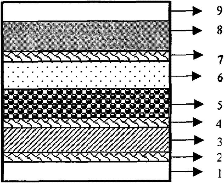
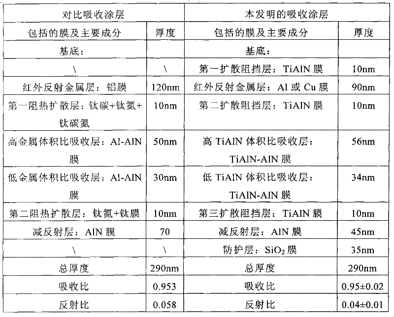
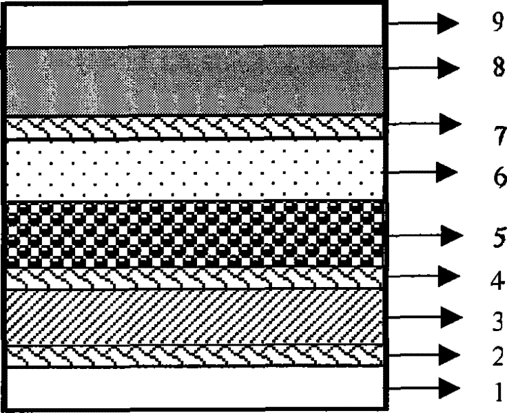
[0055] Using Ti, Al and Cu three-metal targets, and silicon targets, by figure 1 It can be seen that the solar selective absorbing coating of the present invention is divided into 8 layers from the base 1 from bottom to top, which are successively the first diffusion barrier layer 2, the infrared high reflection layer 3, the second diffusion barrier layer 4, and the high nitride conductive particles. Volume ratio absorption layer 5 , low nitride conductive particle volume ratio absorption layer 6 , third diffusion barrier layer 7 , antireflection layer 8 and protection layer 9 .
[0056] Introduce argon gas and nitrogen gas with flow rates of 140SCCM and 20SCCM respectively, use Ti target and Al target for reactive sputtering, the sputtering power of Ti and Al target is 1200w and 800w respectively, to form the first diffusion barrier layer 2 composed of TiAlN, The thickness of this layer is 10 nm;
[0057] The Cu target was non-reactively sputtered in argon to form a Cu thin ...
Embodiment 2
[0066] Using two targets of TiAl alloy and metal Al, as well as a silicon target, by figure 1 It can be seen that the solar selective absorbing coating of the present invention is divided into 8 layers from the base 1 from bottom to top, which are successively the first diffusion barrier layer 2, the infrared high reflection layer 3, the second diffusion barrier layer 4, and the high nitride conductive particles. Volume ratio absorption layer 5 , low nitride conductive particle volume ratio absorption layer 6 , third diffusion barrier layer 7 , antireflection layer 8 and protection layer 9 .
[0067] A TiAl alloy target is reactively sputtered in a mixed gas of argon and nitrogen, the flow rates of argon and nitrogen are 150SCCM and 10SCCM respectively, and the sputtering power of the TiAl target is 1200w to form the first diffusion barrier layer 2 composed of TiAlN. The thickness is 10nm;
[0068]The Al target was non-reactively sputtered in argon to form an Al thin film, th...
PUM
| Property | Measurement | Unit |
|---|---|---|
| thickness | aaaaa | aaaaa |
| thickness | aaaaa | aaaaa |
| thickness | aaaaa | aaaaa |
Abstract
Description
Claims
Application Information
 - R&D Engineer
- R&D Manager
- IP Professional
- Industry Leading Data Capabilities
- Powerful AI technology
- Patent DNA Extraction
Browse by: Latest US Patents, China's latest patents, Technical Efficacy Thesaurus, Application Domain, Technology Topic, Popular Technical Reports.
© 2024 PatSnap. All rights reserved.Legal|Privacy policy|Modern Slavery Act Transparency Statement|Sitemap|About US| Contact US: help@patsnap.com


