
P-type one time programmable (OTP) device and manufacturing method thereof

A manufacturing method and device technology, applied in semiconductor/solid-state device manufacturing, electric solid-state devices, semiconductor devices, etc., can solve the problem of consuming OTP peripheral circuit area, etc.

Active Publication Date: 2011-06-22
SHANGHAI HUAHONG GRACE SEMICON MFG CORP
View PDF0 Cites 12 Cited by
  • Summary
  • Abstract
  • Description
  • Claims
  • Application Information

AI Technical Summary

Problems solved by technology

This will consume a lot of OTP peripheral circuit area
Although the unit area of ​​each P-type OTP device is very small, more peripheral circuits limit the application of this type of device to applications that require high-density capacity

Method used


Image

  • P-type one time programmable (OTP) device and manufacturing method thereof
  • P-type one time programmable (OTP) device and manufacturing method thereof
  • P-type one time programmable (OTP) device and manufacturing method thereof

Examples


Embodiment Construction

[0017] Such as figure 1 Shown is a schematic structural diagram of a P-type OTP device of the present invention, a one-time programmable device formed by connecting a PMOS transistor 11 and a PMOS transistor 12 in series. Wherein the first PMOS transistor 11 is used as a gate transistor, and the source electrode 191 and the drain electrode 192 of the first PMOS transistor 11 are formed in the N-type well 15 with a P-type diffusion region, and its gate 13 is used as the gate of the entire device. line, the source 191 serves as the source of the entire device. The second PMOS transistor 12 is used as the storage unit of the device, and its gate 16 is floating, and the source electrode 192 and the drain electrode 193 of the second PMOS transistor 12 are formed in the N-type well 15 with a P-type diffusion region, so The drain 193 serves as the bit line for the entire device. The source of the second PMOS transistor 12 shares a P diffusion region 192 with the drain of the first ...


PUM


Abstract

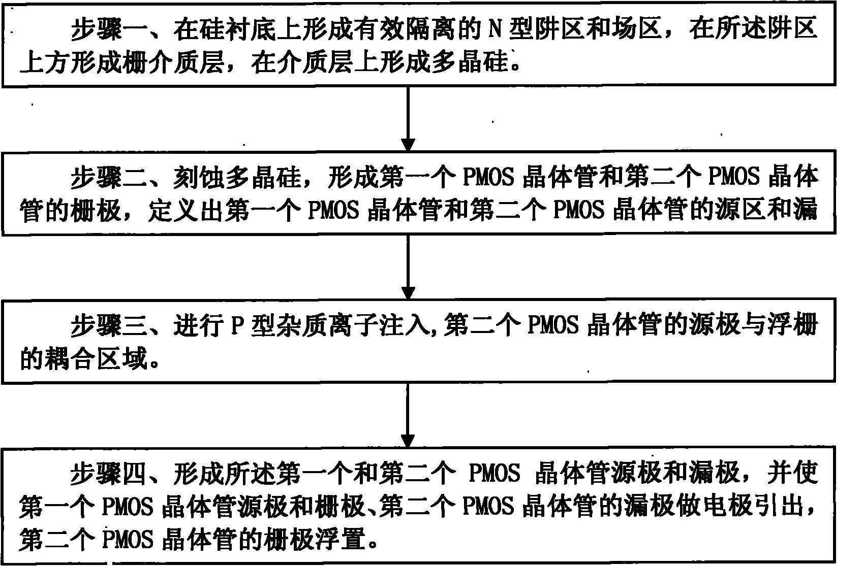
The invention discloses a P-type one time programmable (OTP) device. The device is a one time programmable device formed by two P-channel metal oxide semiconductor (PMOS) transistors connected in series, wherein the first PMOS transistor is used as a gate transistor, while the second PMOS transistor is used as a storage unit, and the grid of the second PMOS transistor floats; and the source of the second PMOS transistor comprises a coupling region of the source and the floating gate formed by injection of P-type foreign ions so as to increase the coupling capacitance between the source and the gate of the second PMOS transistor. The invention also discloses a method for manufacturing the P-type OTP device, which is to form a coupling region of the source and the gate by P-type foreign ioninjection in the second PMOS transistor after polycrystalline silicon is etched. In the invention,, the programming performance of the P-type OTP device is ensured to be greatly improved, the conduction current of the whole device can be improved after programming is completed, the differentiable current ranges of the device before and after programming are increased, and the area of a peripheralcircuit for realizing the OTP function can be reduced.

Description

technical field [0001] The invention relates to the field of manufacturing semiconductor integrated circuits, in particular to a P-type OTP device, and also relates to a method for manufacturing the P-type OTP device. Background technique [0002] The existing P-type OTP device is a one-time programmable device formed by connecting two PMOS transistors in series. The first PMOS transistor is used as a gate transistor, and the source of the first PMOS transistor is formed by using a P-type diffusion region in an N-type well. Pole and drain, the gate of the first PMOS transistor is used as the word line of the entire device, the source of the first PMOS transistor is used as the source of the entire device; the second PMOS transistor is used as the storage unit of the OTP device , the gate of the second PMOS transistor is floating, and the source and drain of the second PMOS transistor are formed in the N-type well with a P-type diffusion region, and the drain of the second PM...

Claims


Application Information

Patent Timeline
IPC IPC(8): H01L27/115H01L21/8247H01L21/8246H01L27/112
Inventor 仲志华
Owner SHANGHAI HUAHONG GRACE SEMICON MFG CORP
Learn More