Method and circuit for processing written address and width unaligned image
A technology of writing address and processing method, which is applied in the field of image processing and processing circuits where the writing address and width are not aligned. problem, to reduce the difficulty of handling, improve flexibility and high efficiency
- Summary
- Abstract
- Description
- Claims
- Application Information
AI Technical Summary
Problems solved by technology
Method used
Image
Examples
Embodiment Construction
[0034] see Figure 1 to Figure 8 As shown, the embodiments of the present invention will be described in detail.
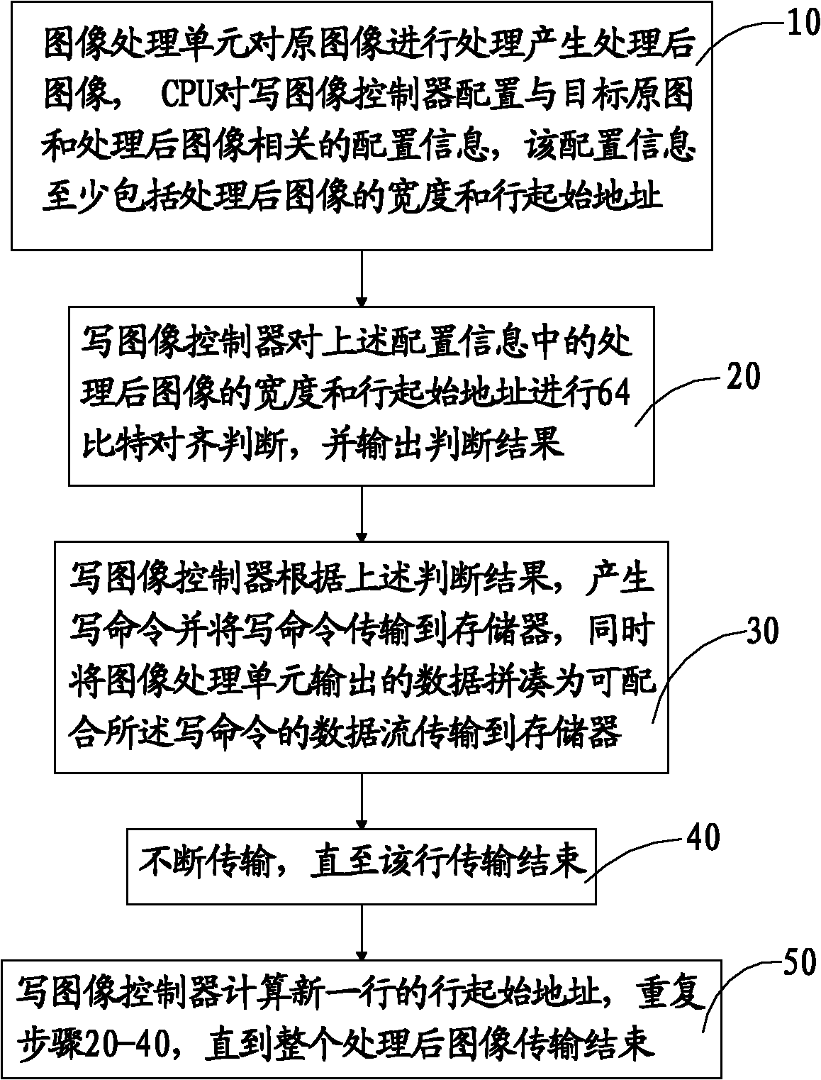
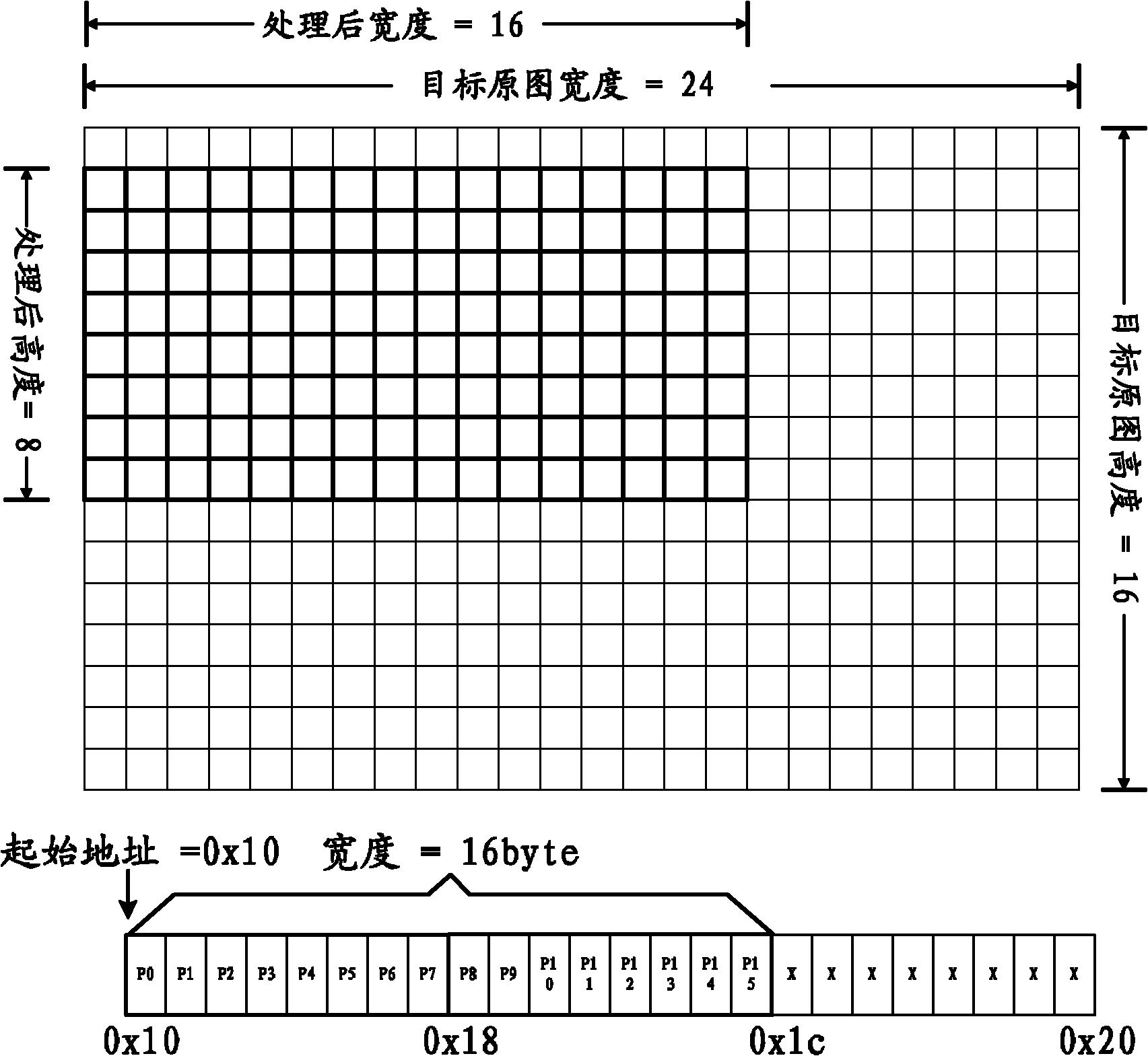
[0035] like figure 1A method of the present invention specifically includes the following steps: step 10, the image processing unit processes the original image to generate a processed image, and the CPU configures the configuration information related to the target original image and the processed image to the image controller, and the configuration The information includes: the format of the transmitted image, the width and height of the original target image, the width and height of the processed image, and the line start address of the processed image; step 20, write the image controller to the width and height of the processed image in the above configuration information The line start address is 64-bit alignment judged, and the judgment result is output, and the judgment result includes: whether the image width is 64-bit aligned, and how much its misalignme...
PUM
 Abstract
Description
Claims
Application Information
 - R&D
- Intellectual Property
- Life Sciences
- Materials
- Tech Scout
- Unparalleled Data Quality
- Higher Quality Content
- 60% Fewer Hallucinations
Browse by: Latest US Patents, China's latest patents, Technical Efficacy Thesaurus, Application Domain, Technology Topic, Popular Technical Reports.
© 2025 PatSnap. All rights reserved.Legal|Privacy policy|Modern Slavery Act Transparency Statement|Sitemap|About US| Contact US: help@patsnap.com


