Chemically mechanical polishing method

A technology of chemical mechanics and polishing time, which is applied in the direction of surface polishing machine tools, grinding/polishing equipment, grinding machine tools, etc., can solve problems such as insufficient wafer polishing, and achieve the goal of reducing labor load, reducing production cycle, and reducing costs Effect

Inactive Publication Date: 2012-12-05
SEMICON MFG INT (SHANGHAI) CORP +1
View PDF0 Cites 0 Cited by
  • Summary
  • Abstract
  • Description
  • Claims
  • Application Information

AI Technical Summary

Problems solved by technology

[0017] In order to be able to effectively solve the problem that the polishing degree of the initial several batches of wafers is not enough after replacing the consumables, the present invention provides a new method for chemical mechanical polishing. The time period when the machine is in the best working condition is defined as the running-in period,

Method used


Image

  • Chemically mechanical polishing method
  • Chemically mechanical polishing method
  • Chemically mechanical polishing method

Examples


Embodiment Construction

[0040] In the following description, numerous specific details are given in order to provide a more thorough understanding of the present invention. It will be apparent, however, to one skilled in the art that the present invention may be practiced without one or more of these details. In other examples, some technical features known in the art are not described in order to avoid confusion with the present invention.

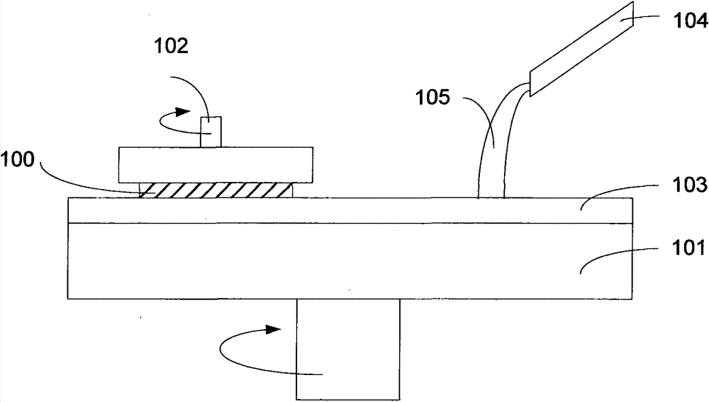
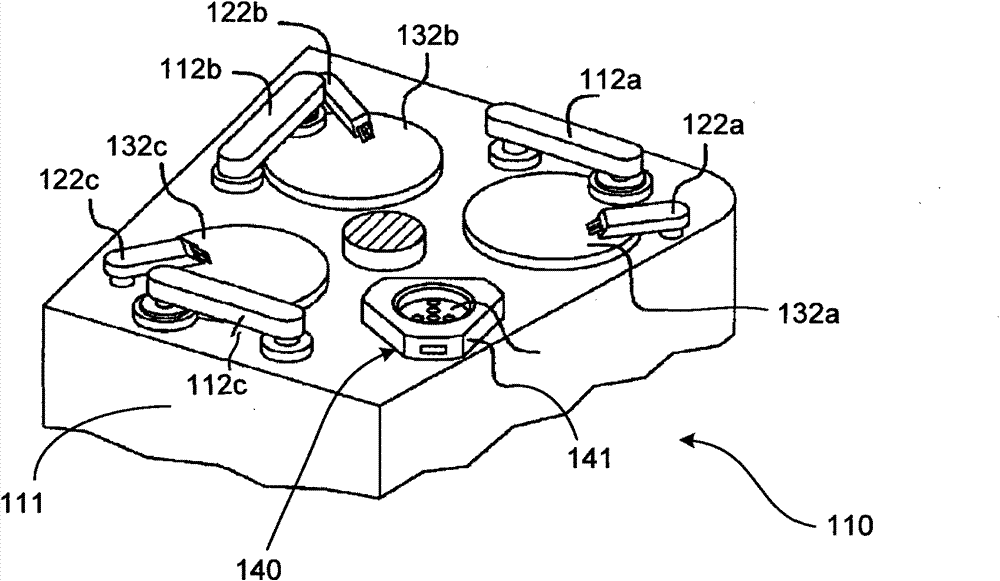
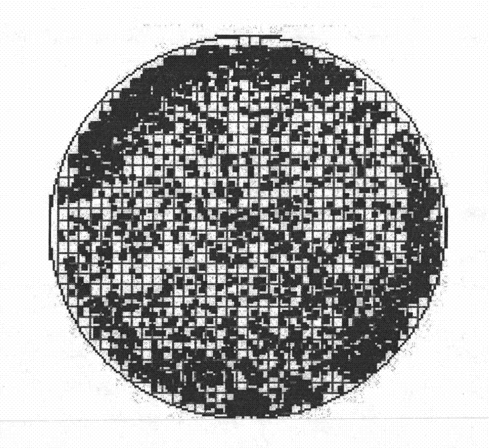
[0041] In order to thoroughly understand the present invention, detailed steps will be proposed in the following description to illustrate how the present invention utilizes the new CMP process to solve the problem of insufficient polishing of the initial batches of wafers after replacing the consumables. Obviously, the practice of the invention is not limited to specific details familiar to those skilled in the semiconductor arts. Preferred embodiments of the present invention are described in detail below, however, the present invention may have other embodim...


PUM


Abstract

The invention discloses a chemically mechanical polishing method. In the method, a time slot from consumable replacement to the optimal operating state of chemically mechanical polishing equipment is defined as a running-in period; and wafers are polished for fixed polishing time in the running-in period, and are polished for unfixed polishing time outside the running-in period. The problem of insufficiency in the polishing degree of a plurality of batches of initial wafers after the consumable replacement can be solved effectively so as to reduce the production cost of semiconductor devices,shorten a production cycle and reduce labor load.

Description

technical field [0001] The invention relates to a semiconductor manufacturing process, in particular to a chemical mechanical polishing method. Background technique [0002] Chemical Mechanical Polishing (CMP) is a common process used to planarize device surfaces. CMP technology is a combination of a rotating platform and a pneumatically driven grinding head. This process basically grinds the front surface of the wafer or the surface of the component to a flat surface in order to prepare for the next step. During this process, the wafer is often ground one or more times in order to make the front surface of the wafer as flat as possible. The wafer is placed in the CMP device with a carrier, and the polished side faces the downward grinding head, which is covered with colloidal silica or alumina grinding liquid. Generally, there are two layers of polishing pads covering the rotating platform, and the outer layer of the polishing pad is an elastic layer. These layers are us...

Claims


Application Information

Patent Timeline
Patent Type & Authority Patents(China)
IPC IPC(8): B24B29/02B24B37/04H01L21/02H01L21/70H01L21/302
Inventor 彭澎
Owner SEMICON MFG INT (SHANGHAI) CORP
Why Eureka
Try Eureka